|
|


 Arabic
 Bengali
 Chinese
 English
 French
 German
 Hebrew
 Hindi
Hindi Italian
 Japanese
 Korean
 Malay
Malay Polish
 Portuguese
 Spanish
 Turkish
 Ukrainian
 Vietnamese
|
ENCYCLOPEDIA OF RADIO ELECTRONICS AND ELECTRICAL ENGINEERING Improvements of the Tselina transceiver. Encyclopedia of radio electronics and electrical engineering
Encyclopedia of radio electronics and electrical engineering / Civil radio communications In order to improve the parameters, the Tselina transceiver [1] was somewhat modified. Applied different RF power amplifier, different power supply, improved front panel design. At the same time, the chassis of the device remained the same, although somewhat modified. The circuit diagram of the power amplifier is shown in fig. 1. The amplifier provides an output power of 10W and is designed to work together with a diode balanced mixer at the input. Despite the high sensitivity, it is resistant to self-excitation, and also produces the same output power regardless of the range, and does not fail when the load is interrupted. The first stage of the amplifier is assembled on a field-effect transistor VT1. Its drain is galvanically connected to the base of the transistor of the second stage VT2. The temperature stability of the second stage is maintained by the first. The third stage is assembled on the KP902 (VT3) transistor. Its gate circuit is powered by +12 V Tx, and the drain-source voltage is +34 V. Fig.1. Schematic diagram of a power amplifier. The fourth stage is VT5 KP901A and VT4 KT922V. The load of the output stage is the step-up transformer Tp1 and then the P-loop. The output impedance of this cascade is significantly higher than that of a cascade made according to a common source circuit. In addition, it is also raised with a step-up transformer Tp1. Such a circuit design made it possible to use a tuned capacitor C16 of a small value of -100 pF at the output. In addition, the quality factor of the output P-loop increased, which led to an increase in the spectral purity of the output signal. Capacitors C1 and C7 remove excess gain in the low bands. Setting up the amplifier comes down to selecting the values of the resistors marked with an asterisk and adjusting the trimming resistor R17 until the modes indicated on the diagram are obtained (in Tx mode with no input signal). In the first stage, the KP305Zh transistor can be replaced by the KP350B transistor, as shown in Fig. 2.
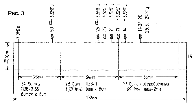
A sketch of the coil of the output circuit is shown in Fig. 3, and the transformer Tp1 is shown in Fig. 4. Details 1...4 in Fig. 4 are made of non-foil fiberglass. Capacitor C16 - type KPV.
The first cascade is made on a printed circuit board, the remaining cascades are hinged in compartments. To connect C16 containers C24...C27 in parallel, an additional biscuit - SJ was used [1, fig. one]. The new amplifier is mounted in the power amplifier compartment, the location of parts is shown in the sketch of the chassis fragment (Fig. 5) Holes were drilled in the transceiver chassis under the ULF board for installing a +34 V stabilizer power transistor. An additional SI U biscuit was installed near the GPA compartment to connect trimmer capacitors to the primary winding of the Tr6 transformer in the drain of the transistor VT8 of the GPA amplifier [1, Fig. 1]. These capacitors, together with the primary winding of the transformer, form resonant circuits, which improves the spectral purity of the VFO signals. Trimmer capacitors are installed on the A13 board. Holes were drilled in the screen partition of the compartment for adjusting the GPA trimmer capacitors. The thermostat board described in [2] is installed in the GPA compartment. An additional RES-78 relay is installed near the GPA capacitor (C22) to receive control voltages of + 12 V Rx, +12 V Tx, as well as to switch the detuning circuits and control the power amplifier. In the compartment of the P-loop, the board of the RF detector A4 and the relay R2 of the RES-9 type, passport RS4.524.202, are installed. As capacitors C23, C24, a variable dual capacitor from the Speedola radio receiver is used. It can be replaced with a capacitor from the Alpinist radio. Drawings of printed circuit boards are shown in fig. 7 ... 15, and the placement of parts on them is shown in fig. 16...24. The printed circuit board of the IF (A2) is designed to install an eight-chip ladder filter at 9 MHz [3]. There are the following inaccuracies in the circuit diagram of the transceiver [1, Fig. 1]:
PCB drawings: Fig.6. UHF and CM N1
Location of elements:
Literature 1. Rubtsov V. Transceiver "Tselina" // Radio amateur. KB and VHF. - 1995. - July. - P.23.
Author: V.Rubtsov (UN7BV); Publication: N. Bolshakov, rf.atnn.ru
The world's tallest astronomical observatory opened
04.05.2024 Controlling objects using air currents
04.05.2024 Purebred dogs get sick no more often than purebred dogs
03.05.2024
▪ Eternal batteries based on nanodiamonds and radioactive waste ▪ Created a unique cold matter ▪ GPS signal will measure wind speed over water ▪ Hockey matches with a first-person view
▪ section of the site Standard instructions for labor protection (TOI). Selection of articles ▪ article I did not pass the academies. I didn't finish them. Popular expression ▪ article Who sailed to Colchis and why? Detailed answer ▪ article Quassia bitter. Legends, cultivation, methods of application ▪ article VHF block (144, 430 MHz). Encyclopedia of radio electronics and electrical engineering
Home page | Library | Articles | Website map | Site Reviews
www.diagram.com.ua |


 Leave your comment on this article: