|
|


 Arabic
 Bengali
 Chinese
 English
 French
 German
 Hebrew
 Hindi
Hindi Italian
 Japanese
 Korean
 Malay
Malay Polish
 Portuguese
 Spanish
 Turkish
 Ukrainian
 Vietnamese
|
ENCYCLOPEDIA OF RADIO ELECTRONICS AND ELECTRICAL ENGINEERING Refinement of the network charger. Encyclopedia of radio electronics and electrical engineering
Encyclopedia of radio electronics and electrical engineering / Chargers, batteries, galvanic cells To use various self-made low-power small-sized devices as built-in power sources, several network chargers for mobile equipment with an output voltage of 5 V at a load current of up to 750 mA were purchased. The specific model name of these devices could not be established, but the boxes were labeled "ILO V3 AMT Style".
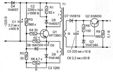
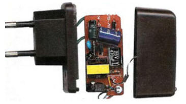
One of them was disassembled (Fig. 1), and according to the printed circuit board and the labeling of the elements on it, its schematic diagram was drawn up, shown in Fig. 2 (the absence of resistor R7 and capacitor C4 on it is explained by their absence on the board). Checking the device for operability showed that with an increase in the load current from 0 to 500 mA, the output voltage decreases from 5,15 to 4,2 V, while the voltage on the capacitor C5 decreases from 7 to 5 V. For testing for long-term operation, the device was loaded current 0,5 A. After about 30 minutes, it failed - the transistor Q1, diode D6, zener diode D8 and resistors R2, R4 turned out to be damaged, while the temperature of the cases of both transistors and transformer T1 reached 80 ... 90 ° C.
In order for such a power supply device to be used for a long time at least at a load current of up to 500 mA, it was modified, as shown in Fig. 3. The numbering of new elements begins with the number 1 and continues the one started in fig. 2. In addition to the inefficient output voltage stabilization unit, made on the elements D6, D8, C6, a stabilization unit has been introduced, consisting of a 1U1 optocoupler, a 1VD9 zener diode and a 1R11 protective resistor. When the output voltage tends to increase, for example, due to a decrease in the load current or an increase in the mains voltage, the current through the emitting diode of the 1U1 optocoupler increases. This leads to the fact that the phototransistor of the optocoupler opens more and shunts the zener diode D8. The output voltage drops. Zener diode D8 is left in the device as a backup loop for stabilizing the output voltage. The transistor voltage regulator on the elements Q2, Q3, R8 is removed. To improve the reliability of the device and improve its performance, the following changes were also made: LC filter 1L11L21C71C8 was introduced, which reduces the level of interference, both coming to the input of the device from the network and in the opposite direction; oxide capacitor C1 is replaced by a larger capacitor and with a higher rated voltage; resistors R2-R4 are replaced by higher resistance resistors; instead of the transistor KF13001 (Q1), a more powerful MJE13003 was used; the diode 1N4007 (D5) was replaced by a high-speed UF4007 (along with an increase in the resistance of the resistor R3, this made it possible to reduce the current consumed by the device from the 1 V network by 220 mA at a load current of 500 mA). In addition, an LC filter 1L31L41C10 is installed at the output of the device. Glowing LED 1HL1 indicates the presence of output voltage. Resistor 1R10 discharges capacitors 1C7, 1C8 after disconnecting the device from the network. Tests of the modified power supply showed that an increase in the load current from 0 to 500 mA causes a decrease in the output voltage from 5,06 to 4,86 V, and the case temperature of the transistor Q1 and transformer T1 does not exceed 55 ° C during long-term operation. The efficiency of the modified device at a load current of 500 mA is 72% (for the original version - 52%). The design uses chokes 1L1 and 1L2 of industrial manufacture, wound on H-shaped ferrite magnetic cores approximately the size of an MLT-0,5 resistor. The resistance of their windings can be from 4 to 50 ohms, inductance - from 22 μH. Capacitors 1C7, 1C8 - ceramic with a rated voltage of 250 V AC or at least 1000 V DC. In the event that the modified device will be operated in the "native" case, the elements 1L1, 1L2, 1C7, 1C8 are mounted in an empty niche where the contact pins for connecting to a power outlet are located. Tests of the modified power supply showed that an increase in the load current from 0 to 500 mA causes a decrease in the output voltage from 5,06 to 4,86 V, and the case temperature of the transistor Q1 and transformer T1 does not exceed 55 ° C during long-term operation. The efficiency of the modified device at a load current of 500 mA is 72% (for the original version - 52%). The design uses chokes 1L1 and 1L2 of industrial manufacture, wound on H-shaped ferrite magnetic cores approximately the size of an MLT-0,5 resistor. The resistance of their windings can be from 4 to 50 ohms, inductance - from 22 μH. Capacitors 1C7, 1C8 - ceramic with a rated voltage of 250 V AC or at least 1000 V DC. In the event that the modified device will be operated in the "native" case, the elements 1L1, 1L2, 1C7, 1C8 are mounted in an empty niche where the contact pins for connecting to a power outlet are located. Capacitors 1C9, 1C10 are ceramic for surface mounting, they are soldered to the pads under the leads of the corresponding oxide capacitors on the side of the printed conductors. Inductors 1L3, 1L4 - with a ferrite magnetic circuit for surface mounting, winding resistance - no more than 0,04 Ohm, inductance - no less than 4,7 μH. The LTV817 optocoupler (it is fixed on the board with Quintol glue) can be replaced with any similar four-pin one, for example, PC817, EL817, PS2501-1, PC814, PC120, PC123 (they have the same pin assignment as LTV817). We will replace the Zener diode BZV55C-4V3 (1VD9) with any similar low-power one with a stabilization voltage of about 4 V at a current of 1 mA. The output voltage depends on the type and instance of this zener diode. If it is necessary to slightly increase the output voltage, the emitting diode of the optocoupler can be shunted with a resistor of several hundred ohms.
Instead of the L-934SGC LED, you can install any ordinary one (without a built-in resistor). Flashing LEDs are not recommended as they may interfere with a nearby radio. Instead of the UF4007 (D5) diode, it is permissible to use MUR160, 1N5398, KD247D, KD258G. We will replace 1N4007 (D4) with the same diodes, in case of damage.
The appearance of the board of the modified device is shown in fig. 4. When setting up and operating the device, remember that most of its elements are under mains voltage, so you must strictly follow the rules of electrical safety. Similarly, other miniature pulse chargers, as well as network adapters, in which there is no feedback on the output voltage, can be modified. Author: A.Butov
Machine for thinning flowers in gardens
02.05.2024 Advanced Infrared Microscope
02.05.2024 Air trap for insects
01.05.2024
▪ Artificial retina will help the blind ▪ A transistor that can be dissolved by sound and water ▪ Microsoft experimental underwater data centers ▪ e-books boom predicted in 2010
▪ site section Parameters, analogues, marking of radio components. Article selection ▪ Article Tomato. Legends, cultivation, methods of application ▪ article Modern silicon photodiodes. Encyclopedia of radio electronics and electrical engineering
Home page | Library | Articles | Website map | Site Reviews
www.diagram.com.ua |


 Leave your comment on this article: