 Free technical library
Modern silicon photodiodes. Reference data

Encyclopedia of radio electronics and electrical engineering / Reference materials
 Comments on the article Comments on the article
This article presents the characteristics of all photodiodes (except for special-purpose devices) produced by Russian enterprises at the present time.
Recall that the photodiode can operate in two modes - photogenerator and photodiode. In the first of them, the device, when illuminated, generates photoEMF, like a solar cell, and in the second, which is used most often, a small closing (reverse) voltage is applied to it and it works as an element, the current through which depends on the intensity of the received radiation and little depends on the applied voltage.
In the drawings, everywhere the letter a (anode) denotes the output from the region p, and the letter k (cathode) - from the region of the n-p-n-junction. The working (reverse) voltage to the photodiode is supplied positively to the cathode.
KDF101A
Photodiodes KDF101A of p-n structure are designed in a semi-cylindrical plastic case with hard tinned leads (Fig. 1).

A photosensitive element measuring 4,5x3,2 mm is located on the side of the frontal plane of the housing. The output broadened near the body is connected to the anode of the photodiode. Weight of the device - no more than 0,25 g.
Photodiodes are designed to work in a remote control system for VCRs and TVs.
- Photocurrent, µA, not less, at illumination 0,5 mW/cm2 at a wavelength of 0,87 µm and a reverse voltage of 5 V......20
- Dark current, nA, no more, at reverse voltage 10V......30
- Spectral photosensitivity area, µm....0,7...1,1
- Rise and fall time of the photocurrent pulse, μs, no more, at a photocurrent of 25 μA and a load resistance of 1,1 kOhm ...... 0,35
- The highest constant operating (reverse) voltage, V ...... 10
- Working range of ambient temperature, °С.....-60...+70
KDF103A
Photodiodes KDF103A of the pin structure with selective sensitivity to IR radiation are designed in a plastic rectangular case with three flat hard tinned leads (Fig. 2).

The area of the photosensitive element is 10,24 mm2. Weight of the device - no more than 0,5 g.
The anode of the photodiode is connected to pin 2 and the cathode to pins 1 and 3 connected together.
Photodiodes are intended for use in the remote control system of VCRs and other household electronic equipment.
- Current photosensitivity, A / W, not less, with radiation with a maximum spectral distribution at a wavelength of 0,9 μm and a reverse voltage of 10 V ...... 0,25
- Photocurrent, mA, not less, at an illumination level of 100 mW / cm2 with a maximum spectral distribution at a wavelength of 0,9 μm and a reverse voltage of 10 V ...... 2,5
- Dark current, µA, no more, at a reverse voltage of 10 V and an ambient temperature of +25 °С......0,01
- +85 °С......15
- Spectral photosensitivity region, µm. . .0,76...0,96
- Angle of the directivity pattern on the level of 0,5, deg.....±45
- The highest constant operating (reverse) voltage, V, at an ambient temperature of + 35 ° C...... 150
- + 85°C......50
- Ambient temperature operating range, °С -45 ... +85
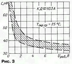
On fig. 3 shows the dependence of the capacitance C of the diode (hereinafter, the graphs show a 95% zone of technological spread; the indicated nature of this dependence is typical for other types of photodiodes, which are described in this article, therefore, these graphs are omitted in the future).
Rice. 4 shows the photosensitivity spectrum of the KDF103A photodiode (here SI OTH equals the ratio of the current photosensitivity to its maximum value).

KDF105A
Photodiodes KDF105A with p-n junction, sensitive to the ultraviolet part of the spectrum, are designed in a glass-to-metal disk case with flexible insulated leads (Fig. 5).

The area of the photosensitive element is 33 mm2. Weight of the device - no more than 3,5 g.
Photodiodes are designed to measure illumination and dosing energy in photometric equipment and process equipment. They can work both in photodiode and photogenerator modes.
The cathode terminal is marked with a black dot on the case.
- Current photosensitivity, A / W, not less, at a reverse voltage of 10 V to radiation at the maximum spectral photosensitivity ...... 0,32
- at a wavelength of 0,254 µm......0,065
- Differential resistance, MOm......80
- Photocurrent pulse rise time, µs, no more, with a load resistance of 10 kOhm......0,1
- 1 kOhm......2
- Photodiode capacitance, pF, max......900
- Spectral photosensitivity area, µm......0,22 ...1,06
- The highest constant operating (reverse) voltage, V ...... 10
- Maximum working illumination, mW/cm2......2
- Working range of ambient temperature, °С.....-60...+50
On fig. Figure 6 shows the spectral monochromatic characteristic of the photosensitivity of KDF105A photodiodes.

KDF110A
KDF110A photodiodes of p-n structure with a photosensitive element area of 9 mm2 are designed in a rectangular plastic case with four rigid stamped tinned leads (Fig. 7).
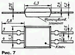
Pin 1 is connected to the anode, 3 and 4 to the cathode; 2 - free. The mass of the device is more than 0,13 g.
Photodiodes are intended for use in medical and other photoelectronic equipment.
- Photocurrent, µA, not less than, at illumination 1 mW/cm2 with a maximum spectral distribution at a wavelength of 0,87 µm and a reverse voltage of 5 V......35
- Monochromatic current photosensitivity, A/W, not less, at a reverse voltage of 5 V and irradiation with a wavelength of 0,93 μm ...... 0,5
- 0,66 µm......0,3
- Temperature coefficient of current photosensitivity, %/°С, not more than......0,5
- Dark current, µA, no more, at a reverse voltage of 10 V and an ambient temperature of +25 °С......0,1
- +55 °С......10
- Rise (fall) time of the photoresponse signal, µs, no more, at a reverse voltage of 10 V and a load resistance of 1 kOhm ...... 1
- Insulation resistance output-housing, MΩ, not less......100
- Photodiode capacitance, pF, no more, at reverse voltage 3 V......75
- The highest constant operating (reverse) voltage, V ...... 15
- Working range of ambient temperature, °С.....-10...+55
A typical spectral characteristic of photosensitivity in relative units of KDF110A photodiodes is shown in fig. 8.

КДФ111А- КДФ111В, КДФ111А1-КДФ111В1
Photodiodes with selective spectral photosensitivity KDF111A, KDF111B, KDF111V have a pin structure, and KDF111A1, KDF111B1, KDF111V1 - p-n. The photosensitive element of the devices is square, 3x3 mm in size.
They are packaged in a drop-shaped plastic case with hard stamped tinned leads (Fig. 9).

The input of radiation - from the side of the lens, along the optical axis. The cathode terminal is marked with a colored dot on the case. The type of device is indicated on the group container. Photodiode weight - no more than 0,5 g.
Designed for use in the system of remote control of household and industrial equipment.
- Photocurrent, µA, not less, at illumination 100 µW/cm2 with a maximum spectral distribution at a wavelength of 0,85 µm and a reverse voltage of 2,5 V for KDF111A......5
- typical value......6,5
- KDF111B......7
- typical value......9
- KDF111V......9
- typical value......10
- Current photosensitivity, A / W, not less, to radiation with a maximum spectral distribution at a wavelength of 0,85 μm at a reverse voltage of 2,5 V for KDF111A1 ...... 0,3
- KDF111B1......0,5
- KDF111V1......0,6
- Dark current, μA, no more, at a reverse voltage of 5 V and an ambient temperature of 25 ° C or less ...... 0,1
- typical value......0,01
- +55 °С for KDF111А......1
- КДФ111А1 - КДФ111В1......5
- +85 °С for KDF111B, KDF111V......10
- Spectral photosensitivity region, µm, for KDF111A-KDF111V .0,76...0,96 KDF111A1-KDF111V1.....0,7...1
- Photodiode capacitance, pF, not more than, at a frequency of 1 MHz for KDF111A (with a reverse voltage of 5 V)...... 70
- KDF111B, KDF111V (2,5)......120
- Rise (fall) time of the photocurrent, µs, no more, under irradiation with a maximum spectral distribution at a wavelength of 0,85 µm, a reverse voltage of 5 V and a load resistance of 51 Ohm for KDF111A1, KDF111B1 ...... 0,1
- KDF111V1......0,7
- Directional pattern angle at the level of 0,5, deg., for KDF111A1-KDF111V1......±40
- The highest constant operating (reverse) voltage, V, for KDF111A, KDF111A1 - KDF111V1 ...... 7
- KDF111B, KDF111V......12
- The highest power dissipation, mW, for KDF111 A-KDF111V......10
- Maximum working illumination, mW/cm2......25
- Ambient temperature operating range, °C, for KDF111A, KDF111A1-KDF111V1......-25...+55
- KDF111B, KDF111V .....-60...+85
On fig. 10 shows typical temperature dependences of the limiting operating (reverse) voltage.

The spectral characteristic of photodiodes KDF111A-KDF111 V.KDF111A1-KDF111V1 is shown in fig. eleven.

KDF115-A, KDF115-AZ, KDF115-A5
Photodiodes KDF115-A, KDF115-AZ, KDF115-A5 with p-n junction are made on the basis of high-resistance silicon. The devices are designed in a plastic case with a lens - KDF115-A (Fig. 12, a) - and with a built-in optical filter to increase protection against radiation in the visible part of the spectrum - KDF115-AZ and KDF115-A5 (Fig. 12, b). In both versions, the terminals are stamped hard tinned.

For KDF115-A devices, the cathode terminal is elongated, and for KDF115-AZ, KDF115-A5, it is broadened at the base. The weight of the photodiode KDF 115-A is 0,24 g, and the rest is 0,4 g. .
Photodiodes are designed to work in the remote control system of equipment, as well as sensors in automation, lighting and signaling devices.
- Current photosensitivity, μA/lx, not less, at reverse voltage 5 V and load resistance 100 Ohm for KDF115-A......0,03
- typical value......0,042
- KDF115-AZ......0,04
- typical value .....0,056
- KDF115-A5......0,09
- typical value......0,11
- Dark current, nA, no more, at a reverse voltage of 5 V at an ambient temperature of +25 °C for KDF115-A......1
- typical value......0,1
- typical value at ambient temperature +70°С ...20
- KDF115-AZ, KDF 115-A5......100
- typical value......10
- typical value at ambient temperature +70°С . .1000 Photodetector time constant, µs, not more than.......0,5
- Spectral photosensitivity region, µm, for KDF115-A......0,4.-1,12
- КДФ 115-АЗ, КДФ115-А5......0,71.-1,12
- Diode capacitance, pF, at a reverse voltage of 5 V for KDF115-A......2,2
- KDF115-AZ, KDF115-A5 .....60
- Wavelength of the maximum spectral distribution of photosensitivity, µm......0,85
- Directional pattern angle at the level of 0,5, deg., for KDF115-A......±5
- KDF 115-AZ......±62
- KDF115-A5......±42
- The highest constant operating (reverse) voltage, V, for KDF115-A, KDF115-A5......50
- KDF115-AZ......30
- Working range of ambient temperature, °С....-60...+70
On fig. 13 shows typical dependences of the current photosensitivity of photodiodes on the operating (reverse) voltage.

Typical spectral characteristics of photodiodes KDF115-A, KDF115-AZ and KDF115-A5 are shown in fig. 14.

KDF118A
Photodiodes KDF118A of p-n structure with selective photosensitivity to IR radiation have photosensitive element dimensions of 5,6x3,4 mm. They are packaged in a plastic case with five rigid stamped tinned leads (Fig. 15).

Pins 1 and 2 are connected to the anode, 4 to the cathode; screen output - 5, output 3 - free. Weight of the device - no more than 0,8 g.
Devices are intended for systems of remote control of the equipment of household and national economic purpose.
- Photocurrent, μA, not less than, at illuminance of 1 mW/cm2 with a maximum spectral distribution at a wavelength of 0,87 μm and an operating (reverse) voltage of 10 V ...... 100
- Dark current, nA, no more, at a reverse voltage of 10 V and an ambient temperature of +25 °С......100
- +55 °С......230
- Rise (fall) time of the photoresponse signal, µs, no more, with irradiation at a wavelength of 0,87 µm, a reverse voltage of 10 V and a load resistance of 1 kOhm......1
- Photodiode capacitance, pF, no more, at reverse voltage 3 V......160
- The highest constant operating (reverse) voltage, V ...... 15
- Working range of ambient temperature, °С.....-60...+55
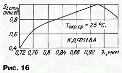
On fig. 16 shows the spectral characteristic of the photosensitivity of the KDF118A photodiode.
COF119A, COF119B
Photodiodes KOF119A, KOF119B with a pn-junction have a photosensitive element area of 40 mm2. They are designed to work in remote control systems, in devices for counting money. Made in a rectangular plastic case with stamped hard tinned leads (Fig. 17). Weight - no more than 0,8 g.

- Current photosensitivity, µA/lx, not less, at operating (reverse) voltage 3 V......0,17
- Dark current, μA, no more, at an operating (reverse) voltage of 3 V ...... 0,5
- Rated illumination during measurements, lx......1000
- Wavelength of the maximum spectral distribution of photosensitivity, µm......0,87...0,96
- The highest constant operating (reverse) voltage, V ...... 10
- Working range of ambient temperature, °С.....-10...+60
COF120A, COF120B; COF121A, COF121B
Photodiodes of the p-n structure KOF120A, KOF120B, KOF121A, KOF121B have a photosensitive element area of 68 mm2 (for KOF120A, KOF120B) and 35 mm2 (KOF121A, KOF121B).
The devices are produced in a plastic case with rigid stamped tinned leads (KOF120A, KOF120B - Fig. 18, a; K0F121A, K0F121B - Fig. 18, b). Weight - no more than 3 g. The cathode lead is broadened at the base.

The main area of application is photosensitive sensors in remote control devices for electronic equipment.
- Current photosensitivity, µA/lx, not less, at operating (reverse) voltage of 3 V for KOF120A, KOF120B ...... 0,32
- KOF121A, KOF121B......0,2
- Dark current, µA, no more, at operating (reverse) voltage of 3 V for KOF120A, KOF120B......1
- typical value......0,5
- KOF121A, KOF121B......0,1
- typical value......0,05
- Rated illumination, lx......1000
- Wavelength of the maximum spectral photosensitivity, µm......0,87...0,96
- The highest constant operating (reverse) voltage, V, for KOF120A, KOF120B......15
- KOF121A, KOF121B......12
- Ambient temperature operating range, °С -10...+60

COF122A, COF122B
Photodiodes of the p-n structure KOF122A, KOF122B with a photosensitive element area of 86 mm2 are designed in a cylindrical plastic case with rigid stamped tinned leads (Fig. 19), the cathode lead is elongated. Weight - no more than 4 g.

Designed for use in remote control systems and other photoelectronic devices.
- Current photosensitivity, μA/lx, not less, at operating (reverse) voltage 12 V, for KOF122A ...... 0,45
- KOF122B......0,3
- Dark current, μA, no more, at an operating (reverse) voltage of 12 V ...... 0,5
- Rated illumination (during measurements), lx......1000
- Time constant of the photodetector, µs, no more......1
- Photodiode capacitance, pF, no more, at operating (reverse) voltage 12 V......600
- Wavelength of the maximum spectral distribution of photosensitivity, µm......0,75...0,85
- The highest constant operating (reverse) voltage, V ...... 30
- Maximum working illumination, lux ...... 1100
- Working range of ambient temperature, °С.....-60...+75
FD-7K gr.A, FD-7K gr.B, FD-24K, FD-24-01
Photodiodes FD-7K gr.A and gr. B, FD-24K and FD-24-01 have a round photosensitive element with a diameter of 10 mm. The device is designed in a cylindrical glass-to-metal case with a flat inlet window, and the outputs are rigid, stamped, tin-plated (Fig. 20).

Marked with colored dots on the case at the cathode terminal. FD-7K gr. A is marked with one black dot, FD-7K gr.B - with one red dot, FD-24K - with one black dot, FD-24-01 - with two black dots, but the latter two have their abbreviated names additionally marked on the case - "24K" and "24 -01". Weight of the device - no more than 10 g.
Photodiodes are widely used in photoelectronic automation.
- Current photosensitivity, μA/lx, not less, at operating (reverse) voltage of 27 V and illumination of 1000 lx for FD-7K gr.A, FD-7K gr.B ..... 0,56
- FD-24K ...... 0,47
- FD-24-01......0,15
- Dark current, µA, no more, at operating (reverse) voltage 27 V for FD-7Kgr.A, FD-7Kgr.B......5
- FD-24K, FD-24-01......2,5
- Noise voltage, μV / Hz0,5, not more, at an operating (reverse) voltage of 27 V for FD-7K gr.A in the absence of radiation ..... 0,61
- with radiation with an illumination of 1000 lux ...... 4,2
- Time constant of the photodetector, µs, no more......10
- Photodiode capacitance, pf, no more, at operating (reverse) voltage 27 V......600
- Spectral photosensitivity region, µm.....0,4...1,1 Wavelength of maximum spectral distribution of photosensitivity, µm, for FD-7Kgr.A, FD-7Kgr.B .0,82...0,86
- ФД-24К, ФД-24-01.....0,75.-0,85
- The highest constant operating (reverse) voltage, V ...... 30
- Maximum working illumination, lx......1100
- Maximum short-term (no more than 2 min) illumination, lux ...... 11 000
- Working range of ambient temperature, °С.....-60...+75
On fig. 21, a and b show typical spectral characteristics of photodiodes.

FD-8K gr. 1690, FD-8K gr. 1691
Photodiodes FD-8K gr.1690 and FD-8K gr.1691 of the p-n structure with a photosensitive element 2x2 mm in size are designed in a metal-glass case with flexible insulated tinned leads (Fig. 22); weight - no more than 1 g.

Devices are marked with colored annular stripes on the body, FD-8K gr.1690 - one, and FD-8K gr.1691 - two. The former are designed to operate in the photodiode mode, and the latter in the photogenerator mode. At FD-8K gr.1690, the cathode lead is extended, auFD-8Kgr.1691 - the anode.
The devices are widely used in photoelectronic automation.
- Current photosensitivity, μA/lx, not less than, at illumination 1500 lux and rated operating voltage for FD-8K gr.1690......6-10-3
- FD-8K gr.1691......4,2-10-3
- Rated operating (reverse) voltage, V, for FD-8K gr.1690......20
- FD-8K gr.1691......0
- Dark current, µA, not more, at reverse voltage 20 V and ambient temperature +25 °С for FD-8K gr.1690......1
- FD-8K gr.1691......3*
- Dark current, µA, not more, at reverse voltage 20 V and ambient temperature +85 °С for FD-8K gr.1690......2
- FD-8Kgr. 1691......7*
- Photoresponse signal rise time, µs, no more, for FD-8K gr.1690......7,5
- FD-8K gr.1691......12
- Spectral photosensitivity area, µm.....0,5...1,12
- Wavelength of the maximum spectral distribution of photosensitivity, µm......0,85...0,92
- The highest constant operating (reverse) voltage, V, for FD-8K gr.1690......30
- Maximum working illumination, lx......2000
- Working range of ambient temperature, °С.....-60...+85
* Reference values.
FD-263, FD-263-01
Photodiodes FD-263, FD-263-01 of p-n structure have a photosensitive element 3x3 mm in size.
Devices FD-263 are designed in a glass-to-metal case with a flat input window and rigid tinned wire leads, and FD-263-01 - in a plastic case with a window in the form of a spherical lens and hard stamped tinned leads (Fig. 23, a and b, respectively). Weight of FD-263 - no more than 3 g, and FD-263-01 -2 g.

The cathode terminal of the FD-263 device is marked with a black dot on the case, while that of the FD-263-01 is elongated. Photodiode FD-263 is designed to operate in photogenerator mode, and FD-263-01 - in photodiode mode.
The devices are widely used in various photoelectronic assemblies and devices.
- Integral current photosensitivity, µA/lx, not less, at reverse voltage 12 V for FD-263......0,18*
- FD-263-01......0,12
- Rated operating voltage, V, for FD-263......0
- FD-263-01......12
- Dark current, nA, no more, at a reverse voltage of 12 V for FD-263......5*
- FD-263-01......100
- Photodetector time constant, µs, not more than .. . .0,02 Spectral photosensitivity region, µm.....0,4... 1,1
- The highest constant operating (reverse) voltage, V ...... 30
- Working range of ambient temperature, °С.....-50...+50
* Reference values.
ФД-265А, ФД-265-01А, ФД-265-02А,ФД-265Б, ФД-265-01Б
Photodiodes FD-265A, FD-265-01A, FD-265-02A, FD-265B, FD-265-01B of p-n structure have a photosensitive element area of about 2 mm2, and for FD-265A and FD-265B it is round with a diameter 1,37 mm, and the rest - square with dimensions of 1,4x1,4 mm.
Photodiodes FD-265A and FD-265B are designed in a metal-glass case, the rest are in a plastic case, and for PD-265-01A and FD-265-01B, the case on the side of radiation reception is made in the form of a lens (Fig. 24, a - c) Conclusions for FD-265A, FD-265B, FD-265-01A and FD-265-01B hard wire tinned, and for FD-265-02A - hard stamped tinned. Weight - no more than 1 g.

Part of the FD-265-02A photodiodes was made in a black polymer case. Such devices have somewhat different characteristic values and the region of spectral photosensitivity is shifted towards longer wavelengths.
Devices that have the letter index B in the name are marked with a black dot on the case. These photodiodes are designed to work in the photogenerator mode, but can also be used in the photodiode mode if the operating (reverse) voltage does not exceed 4 V. Devices with index A must work in the photodiode mode.
Designed for use in electronic video and audio equipment.
- Current photosensitivity, µA/lx, not less, at rated operating (reverse) voltage for FD-265A......0,75-10-2
- ФД-265-01А, ФД-265-01Б......2·10-2
- FD-265B ...... 0,6 10-2
- ФД-265-02А......4·10-2
- FD-265-02A black......3,5 10-2
- Rated operating (reverse) voltage, V, for FD-265A......4
- ФД-265-01А, ФД-265-02А......5
- FD-265B, FD-265-01B......0
- Dark current, μA, no more, at a reverse voltage of 12 V and an ambient temperature of +25 ° C for FD-265A ...... 0,1
- FD-265B, FD-265-01B......1*
- FD-265-01A,
- FD-265-02A......5 10-3
- FD-265-02A black ...... Z0 10-3
- Dark current, µA, not more than at reverse voltage of 12 V and ambient temperature of +85°C for FD-265A......2
- FD-265B, FD-265-01B......6*
- ФД-265-01А, ФД-265-02А......1
- FD-265-02A black......2
- Time constant of the photodetector, ms, no more, for FD-265A, FD-265-01A, FD-265-02A ...... 0,05
- FD-265B, FD-265-01B......5
- Spectral photosensitivity area, µm....0,4...1,2
- Wavelength of the maximum spectral distribution of photosensitivity, µm......0,75...0,9
- Angle of the directivity pattern at the level of 0,5, deg., not less......±36
- The highest constant operating (reverse) voltage, V ...... 100
- Maximum working illumination, lx......2000
- The greatest short-term illumination (within 200 hours), lux ...... 45 000
- Working range of ambient temperature, °С.....-60...+85
* Reference values.
On fig. 25a shows the spectral characteristics of the photosensitivity of photodiodes of the FD-265 series, and in fig. 25, b - black photodiode FD-265-02A.

FD-320, FD-320-01
Photodiodes FD-320, FD-320-01 of the p-n structure with a square photosensitive element with an area of 25 mm2 are designed in a plastic case with rigid stamped tin-plated leads. For the FD-320, the entrance window is made in the form of a lens (Fig. 26a). The sensitivity of the device is maximum when the radiation incident on it is directed along the optical axis; FD-320-01 has no lens (Fig. 26b). Weight of the device - no more than 10 g.

Photodiodes are used as infrared radiation sensors in radio electronic equipment remote control systems.
- Current photosensitivity, μA/lx, not less, at operating (reverse) voltage of 10 V for FD-320 ...... 0,15
- FD-320-01......0,035
- Dark current, nA, no more, at operating (reverse) voltage 10V......50
- typical value......2
- Time constant of the photodetector, µs, no more......1
- Photodiode capacitance, pF, no more, at operating (reverse) voltage 10 V......30
- Spectral photosensitivity area, µm.....0,7...1,1
- Wavelength of the maximum spectral distribution of photosensitivity, µm......0,87...0,96
- The highest constant operating (reverse) voltage, V ...... 30
- Working range of ambient temperature, °С.....-60...+85
KFDM, KFDM gr.A, KFDM gr.B
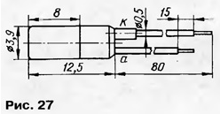
Photodiodes KFDM, KFDM gr.A, KFDM gr.B of the p-n structure with a square photosensitive element measuring 1,9x1,9 mm are designed in a glass-to-metal case with flexible tinned leads (Fig. 27). The cathode lead is extended. Weight - no more than 1 g.
Devices KFDM and KFDM gr.B are designed to operate in the photodiode mode, and KFDM gr.A can be used both in photodiode and photogenerator modes.
Photodiodes are used in various electronic-optical equipment.
- Current photosensitivity, µA/lx, not less, at rated operating voltage and illumination 1500 lux for KFDM......0,75 10-2
- KFDM gr.A ...... 0,8 10-2
- KFDM gr.B......1,5 10-2
- Rated operating (reverse) voltage, V, for KFDM, KFDM gr.B......20
- KFDM gr.A......0
- Dark current, µA, no more, at operating (reverse) voltage of 20 V and ambient temperature of +25°С for KFDM......1
- KFDM gr.A*, KFDM gr.B......0,1
- Dark current, µA, no more, at operating (reverse) voltage of 20 V and ambient temperature of +85°С for KFDM......3,5
- UFDM gr. A*, KFDM gr. B......2
- Photoresponse signal rise time, µs, no more, at operating (reverse) voltage of 20 V and load resistance of 10 kOhm ...... 10
- Spectral photosensitivity area, µm.....0,5... 1,12
- Wavelength of the maximum spectral distribution of photosensitivity, µm......0,85...0,92
- Angle of the directivity pattern at the level of 0,5, deg., not less......±36
- The highest constant operating (reverse) voltage, V, for KFDM......22
- KFDM gr. A, KFDM gr.B......30
- Maximum power dissipation, mW......350
- Maximum working illumination, lx......2000
- Working range of ambient temperature, °С.....-60...+85
* Reference values.
On fig. 28 shows the relative spectral characteristic of photodiodes of the KFDM series

Author: A.Yushin
 See other articles Section Reference materials. See other articles Section Reference materials.
Read and write useful comments on this article.
<< Back
 Latest news of science and technology, new electronics: Latest news of science and technology, new electronics:
Traffic noise delays the growth of chicks
06.05.2024
The sounds that surround us in modern cities are becoming increasingly piercing. However, few people think about how this noise affects the animal world, especially such delicate creatures as chicks that have not yet hatched from their eggs. Recent research is shedding light on this issue, indicating serious consequences for their development and survival. Scientists have found that exposure of zebra diamondback chicks to traffic noise can cause serious disruption to their development. Experiments have shown that noise pollution can significantly delay their hatching, and those chicks that do emerge face a number of health-promoting problems. The researchers also found that the negative effects of noise pollution extend into the adult birds. Reduced chances of reproduction and decreased fertility indicate the long-term effects that traffic noise has on wildlife. The study results highlight the need ... >>
Wireless speaker Samsung Music Frame HW-LS60D
06.05.2024
In the world of modern audio technology, manufacturers strive not only for impeccable sound quality, but also for combining functionality with aesthetics. One of the latest innovative steps in this direction is the new Samsung Music Frame HW-LS60D wireless speaker system, presented at the 2024 World of Samsung event. The Samsung HW-LS60D is more than just a speaker system, it's the art of frame-style sound. The combination of a 6-speaker system with Dolby Atmos support and a stylish photo frame design makes this product the perfect addition to any interior. The new Samsung Music Frame features advanced technologies including Adaptive Audio that delivers clear dialogue at any volume level, and automatic room optimization for rich audio reproduction. With support for Spotify, Tidal Hi-Fi and Bluetooth 5.2 connections, as well as smart assistant integration, this speaker is ready to satisfy your ... >>
A New Way to Control and Manipulate Optical Signals
05.05.2024
The modern world of science and technology is developing rapidly, and every day new methods and technologies appear that open up new prospects for us in various fields. One such innovation is the development by German scientists of a new way to control optical signals, which could lead to significant progress in the field of photonics. Recent research has allowed German scientists to create a tunable waveplate inside a fused silica waveguide. This method, based on the use of a liquid crystal layer, allows one to effectively change the polarization of light passing through a waveguide. This technological breakthrough opens up new prospects for the development of compact and efficient photonic devices capable of processing large volumes of data. The electro-optical control of polarization provided by the new method could provide the basis for a new class of integrated photonic devices. This opens up great opportunities for ... >>
| Random news from the Archive iPhone 6 will be assembled by robots
07.07.2014
Foxconn's program to equip its production lines with robots is nearing its final stage. Initially, 10 robots will be installed. The first devices that Foxconn will trust machines to assemble will be the new-generation iPhones.
According to a company representative, the launch of robots should take place in the near future at one of the enterprises where Apple products are produced. As Terry Gou emphasized, first of all the company is going to use robots for the production of products of the "apple" company. Perhaps the iPhone 6 will be one of the first such products.
Foxconn will initially install 10 robots called Foxbot to replace humans. Each such robot will be able to assemble 30 devices a year. The cost of the robot, depending on the functionality, will be 20-25 thousand dollars.
Foxconn representatives first announced plans to equip their production lines with robotics in 2011. Then Terry Gou said that 10 thousand robots already operate in their factories, and by 2014 their number is planned to be increased to 1 million units.
How many robots are currently present at Foxconn's facilities is unknown. But it is clear that they will not be able to increase production capacity to the required value: in June 2014, the company announced that they were going to hire an additional 100 thousand employees to assemble new iPhones.
Be that as it may, Foxconn expects that replacing people with machines will significantly reduce costs. In addition, the transfer of a number of operations to mechanisms will provide an opportunity to relieve people and, as the company believes, will help improve working conditions. Today, Foxconn employs more than 1,2 million manual assembly workers. The company repeatedly fell under the scope of various human rights organizations due to exceeding the maximum permitted working week (in China it is 49 hours). But that's just one aspect of Foxconn's not-so-clean reputation. In May of this year, it became known that some of the company's employees received multimillion-dollar bribes in exchange for lucrative contracts.
Announcement of the iPhone 6th generation is expected on September 25, 2014.
|
Other interesting news:
▪ Optical gyroscope using rotating light
▪ Acoustic sensors on military helmets will detect snipers
▪ Nanoparticles catch light
▪ The benefits and harms of video games
▪ Application Processors with High-Speed Wireless LAN Module and NAND Flash
News feed of science and technology, new electronics
Interesting materials of the Free Technical Library:
▪ site section Spectacular tricks and their clues. Article selection
▪ Microscope article. History of invention and production
▪ article Where is the Eastern Garbage Continent located? Detailed answer
▪ article by Ferul Karelin. Legends, cultivation, methods of application
▪ article Pinout of all computer connectors. Encyclopedia of radio electronics and electrical engineering
▪ article Radio receiver on the K174XA10 chip. Encyclopedia of radio electronics and electrical engineering
Leave your comment on this article:
 All languages of this page All languages of this page
Home page | Library | Articles | Website map | Site Reviews

www.diagram.com.ua
2000-2024
|


 Arabic
 Bengali
 Chinese
 English
 French
 German
 Hebrew
 Hindi
Hindi Italian
 Japanese
 Korean
 Malay
Malay Polish
 Portuguese
 Spanish
 Turkish
 Ukrainian
 Vietnamese