|
|


 Arabic
 Bengali
 Chinese
 English
 French
 German
 Hebrew
 Hindi
Hindi Italian
 Japanese
 Korean
 Malay
Malay Polish
 Portuguese
 Spanish
 Turkish
 Ukrainian
 Vietnamese
|
ENCYCLOPEDIA OF RADIO ELECTRONICS AND ELECTRICAL ENGINEERING Circuitry of switching power supplies. Encyclopedia of radio electronics and electrical engineering
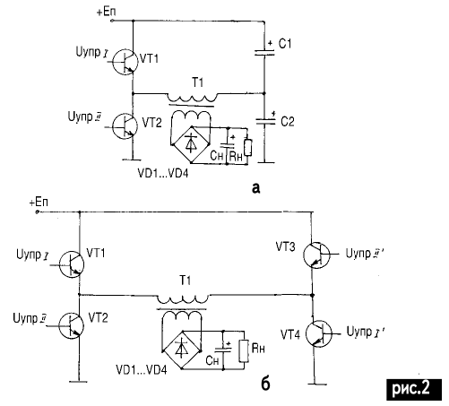
Encyclopedia of radio electronics and electrical engineering / Power Supplies Switching power supplies (UPS) are increasingly used in household and industrial equipment. Modern UPS circuitry is so advanced that it is equal to linear power supplies in terms of the number of elements, and in many respects exceeds linear PSUs. The operation of the UPS in networks where the alternating voltage of 220 V has (in the mode of overload or phase imbalance) a spread of parameters from 160 to 280 V gives a huge advantage over linear power supplies. In addition, high efficiency can significantly reduce energy consumption from the network (which is important for low-income families). Switching power supplies are divided into single-cycle voltage converters (OPN) and push-pull. In turn, single-cycle converters are divided into PN with reverse diode connection (OPNO) (flyback) Fig. 1, a and with direct connection of the OPNP diode (forward) Fig. 1, b.
Push-pull are divided into PN with a half-bridge switching circuit (Fig. 2, a) and with a bridge switching circuit (Fig. 2, b).
According to the analysis carried out in [1], the field of application of the PV depends on the load power (Fig. 3), while the schemes for switching on the PV are different. In imported household equipment, you can most often find a flyback PN circuit, since it has a very small number of elements. But for the normal operation of this circuit, high-quality elements are required that are not available in a wide range on the market of electronic components in Ukraine. The operation of low-quality radio components greatly affects many UPS indicators.
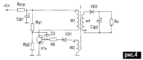
Let's consider the operation of a single-ended voltage converter with a reverse diode connection. They are often called flyback because of the transfer of energy to the load at the moment the transistor key is turned off. Figure 4 shows a simplified diagram of a modern flyback PN.
Period t0 - t1. As soon as the supply voltage + Ep is applied, a current flows through Rogr, RD1, RD2, while C3 is charged with current through Rogr, Rd1, C3, the B-E junction of the transistor VTk (Fig. 5, a). Transistor VTk gradually opens t0 t1 (Fig. 5, b), a collector current IKVT arises (Fig. 5, c), flowing along the path: + En, Rogr, w1, the E-B transition of the transistor VTk - ground. On the winding w2, an EMF of the same polarity is induced as the voltage applied to w1, according to the law of self-induction (the beginning of the point on the windings). The self-inductance emf is applied with a plus through VD1, Rb to the B-E VTk junction, the transistor unlocks even more.
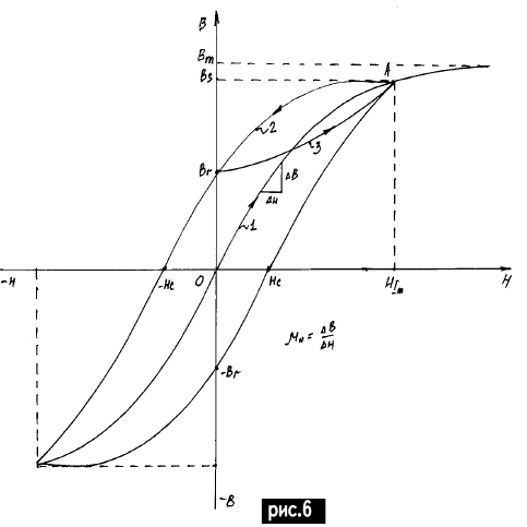
Note that no current flows in the load circuit. The collector circuit current VTk increases until the transistor saturates, while the inductor current in w1 increases from zero to ILmax, and while the collector current changes and grows, the inductor core L is magnetized. Figure 6 shows a hysteresis loop. Since the magnetic field strength is directly proportional to the current flowing in the winding w1, Iw1 \u6d Hl / w, where H is the magnetic field strength; l is the path length of the magnetic line; w is the number of turns, then the magnetic field strength in the inductor core will also gradually increase from zero to HIm (Fig. 1, curve XNUMX).
Period t1 - t2. At the moment of saturation of the transistor VTk (note that this moment does not coincide with the moment of saturation of the core due to the design features of the circuit), the collector current of the transistor VTk reaches its maximum value (all the main carriers of the n-p-n junction are involved) and does not change. In w1, the inductor current also does not change, which means that no more self-induction EMF is induced in w2. In this case, VTk is locked. The inductor core L begins to demagnetize, the energy of the core is transferred to the load, since the self-induction EMF reverses polarity at w3. In this case, a current appears in w3 through VD2 and Rn, Cf. Since the EMF has changed sign, no current flows in w2, and VTk finally closes. C3 is already charged and VTk cannot open. The demagnetizing current Im gradually decreases t1 t2 (Fig. 5d). The magnetic field strength also gradually decreases from point A to point Br (Fig. 6, curve 2). The capacitor SF2 quickly charges, and the load current flows through Rn. As soon as the field strength drops to zero, the current in w3 stops, the core has a residual value of the magnetic field induction Br, so the core is not completely demagnetized (for complete demagnetization, it is necessary to apply a coercive force, -Nc. In push-pull bridge or half-bridge circuits, the core is demagnetized and remagnetized opposite arm of the circuit This feature is very important when calculating the inductor, since Bm (the amplitude value of the induction in the formulas) will be 60-80% less (depending on the quality of the core) of the tabular value. Period t2 - t3. As soon as the inductor core is demagnetized to the residual value Br, while the magnetic field strength does not change and is equal to zero, the current in w3 stops flowing, and the EMF in w2 changes sign to the opposite, VTk begins to open with the base current, as a result, the collector current VTk increases, increasing EMF on w2 by increasing the current through w1. Transistor VTk opens to saturation (Fig. 5c), the core is magnetized (Fig. 6, curve 3), at point A for HIm the induction value BS will correspond. In calculations, instead of Bm, the difference ∆B = Bs - Br is used, i.e. the converter operates on a private hysteresis loop. Therefore, in single-ended voltage converters, ferrites with a minimum Br and a maximum Bs (narrow hysteresis loop) are used. A similar loop exists in high-frequency ferrites, so many foreign companies create converters with a conversion frequency from 0,1 to 1 MHz. The operation of the converter at such a frequency requires the use of high-quality RF elements (power). It is important to note that the duration of the open state VTk is determined by the amplitude of the collector current Ikmax, the inductance L and the voltage of the power supply Ep and does not depend on the output load. The duration of the closed state directly depends on the load. Therefore, there are three modes of operation of the PN. 1st intermittent current mode The load resistance is small (almost a short circuit and the capacitor SF2 does not have time to charge, while voltage and current ripple will be observed on Rn. 2nd continuous current mode Sf will accumulate enough energy so that the current in the load flows without ripples, and the voltage is constant. 3rd mode for OP only BUT - idle mode. The load is insignificant or completely disconnected, the duration of the closed state of the transistor increases (due to the slow decrease in the demagnetization current), but since the energy stored in the magnetic field of the transformer does not change, the voltage on the secondary winding, and therefore on the load, increases to infinity . This mode is the most dangerous, since SF2 can explode from overvoltage. Therefore, in no case should flyback voltage converters be used in the cold mode. (with the exception of laser systems, photo flashes, medical high voltage storage devices). Flyback chokes cores PN. Cores are mainly made from ferrites. Ferrites are a sintered mixture of ferric oxide with oxides of one or more divalent metals [2]. Ferrites are very hard, brittle and similar in mechanical properties to ceramics (mostly dark gray or black in color). The density of ferrites is much less than the density of metallic magnetic materials and is 4,5-4,9 g/cm3. Ferrites are well ground and polished with abrasive materials. They can be glued with BF-4 glue according to a well-known technology (clean with sandpaper, degrease with gasoline, apply glue and let dry a little, squeeze firmly with a press for several hours, but so as not to split the ferrite). Ferrites are semiconductors and have electronic conductivity. Their resistivity (depending on the brand) ranges from 10 to 1010 ohm x cm Table 1
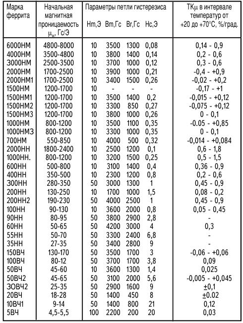
The main characteristics of ferromagnetic materials are given in Table 1:
Modern soft magnetic ferrites can be divided into several groups that differ in electromagnetic parameters and purpose. In the designation of the ferrite grade, the numbers correspond to the nominal value of the initial magnetic permeability, the first letter H means that the ferrite is low-frequency, the second letter M is manganese-zinc ferrite, H is nickel-zinc; the letters HF indicate that the ferrite is designed to operate at high frequencies. Ferrites grades 6000NM, 4000NM, 3000NM, 2000NM, 1500NM, 1000NM are used at frequencies up to several hundred kHz in both weak and strong fields. In weak fields, ferrites of this group are used in cases where there are no increased requirements for temperature stability. Ferrites of the first three grades are recommended to be used in magnetic cores instead of sheet permalloy with a thickness of 0,1-0,02 mm or less. Ferrites grades 2000NM1, 1500NMI, 1500NM2, 1500NM3, 1000NM3 and 700NM are designed for use in weak and medium fields at frequencies up to 3 MHz. They have low losses and low TCµ over a wide temperature range. With increased requirements for thermal stability µ in a wide temperature range, it is preferable to use ferrites of the last three grades. Ferrites grades 2000NN, 1000NN, 600NN, 400NN, 200NN and 100NN are used in weak fields in the frequency range up to several MHz. Ferrites of the first three grades are significantly inferior to manganese-zinc ferrites with the same values of µ, but they are cheaper, therefore they are widely used in various equipment with low requirements for stability and losses. The remaining ferrites are widely used in circuit coils and magnetic antennas. Ferrites grades 150VCh, 100VCh, 50VCh2, 30VCh2 and 20VCh are designed for use in weak fields at frequencies up to 100 MHz. They are characterized by low losses and low TKµ over a wide temperature range, therefore they are most widely used for high-frequency inductors, as well as for antennas of portable radio receivers. Ferrites of grades 300НН, 200НН2, 150НHI, 90НН, 60НН, 55НН, 33НН and 10ВЧ1 are characterized by low losses in strong fields. Their main purpose is for coil cores of circuits tunable by biasing, and circuits of magnetic modulators. In weak fields tanδ and TKµ, these ferrites are much more numerous than ferrites of the HF group. The main data of soft magnetic ferrites are given in Table 2. Conversion units for the SI system: 1 Gs-10-4 Tl. Table 2
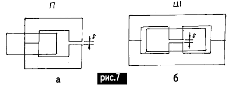
Flyback PN cores are made in the form of U-shaped or W-shaped magnetic circuits (Fig. 7).
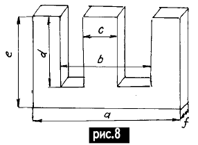
Since the transformer acts as a choke, one of the sides of the core is filed with abrasive material (preferably with a diamond file). The non-magnetic gap is performed within 0,1 ... 0,3 mm, cardboard is inserted into the gap during assembly. The most common overall dimensions of W-shaped magnetic circuits are given in Table 3 and in Fig. 8. Table 3
Calculation of flyback chokes PN The inductor core must store the required peak energy in a small gap without entering saturation and have acceptable losses in the magnetic circuit. In addition, it must accommodate the required number of turns to provide acceptable winding losses. We use the well-known formula [3]: Pgab = IkUk = 4fwkBmSc10-4Ik; (one) Uk = 4fwkBmSc10-4, (1a) where Rgab is the overall power of the transformer, W; Ik - average collector current, A; Uk - voltage applied to the primary winding of the inductor, V; f - conversion frequency, Hz; Bm - magnetic field induction, T (for single-cycle PN Vm \u0,7d Bs - Br is approximately 2 of the table value); Sc - cross-sectional area of the magnetic circuit rod, cmXNUMX; wk is the number of turns of the primary winding. From (1) it follows that the number of turns of the primary winding can be found as follows: w1 = 0,25Uk104/(fBmSc). (2) Choke inductance: L = µ0 µr (w1)2 Sc/l, (3) where L - inductance, H; µ0 = 4π10-7 - absolute magnetic permeability; µr - relative magnetic permeability; Sc - cross-sectional area of the magnetic core, m2; l is the path length of the magnetic line, m. For a rough estimate of the required core cross section, you can use the expression: Sc = (10...20) (Pn/f)1/2(4) where Pn - load power, W; Sc - cross-sectional area of the core, cm2; f - conversion frequency, Hz. Using formulas (2) and (4), as well as analyzing the data in Table 2, we find the overall dimensions of the core and the number of turns of the primary winding. For the secondary and other windings wн = w1 Uk/Uн, where Un is the load voltage. For the excitation winding w2 (see Fig. 4), a voltage of approximately 5 V is recommended. Wire diameter d = 1,13 (I/j)1/2(5) where d - wire diameter, mm; I - average current in the winding, A; j is the current density in the winding (recommended 2,5...5 A/mm2), and for the internal winding the current density should be the lowest. To check the calculations, we calculate the area occupied by each winding and summarize, while the inequality must be satisfied: Sok = w1d1 + w2d2 + w3d3 + ... + wndn + hz, (6) where Sok is the tabular value of the window area, cm2; wn number of turns in winding n; dn is the diameter of the wire in the winding n; hz is the total thickness of the frame and winding insulation. The frames on which the windings of transformers are wound are pressed from plastics, glued from electric cardboard or assembled from separate parts made of layered textolite, pressboard or electric cardboard, with small dimensions, any cardboard is used. The standard manufacture of a cardboard frame is described in detail in [4], for transformers of small power, the author proposes a second method for manufacturing a transformer (Fig. 9). It consists of three blanks. The sleeve is made of cardboard (Fig. 9, b), the lines 1 of the workpiece are slightly cut, after which it is folded into a parallelepiped and the edges 2 are glued along the contour 3 with tissue paper. The blank (Fig. 9, a) is made in the amount of 2 pcs. At the same time, core 1 is cut out and holes D0,3 mm are pierced with a needle sharpened along the edges from a syringe, after which they are numbered (on the upper half of the frame as H1, H2, H3, ..., and on the lower half as K1, K2, K3 , ...). The upper and lower halves of the frame are glued to the sleeve with tissue paper and the structure is left under a heavy object for several hours. The winding of the windings on the frame is carried out similarly to [4] in the following order Wcontrol, W1, Wload (for experimental options, Wcontrol can be the last one).
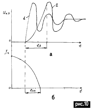
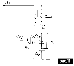
Assembly Ferrite rods are inserted into the frame with wound windings. First, a cardboard square 0,2 mm thick is glued to one of the cores to fill the gap. After assembling the core from the side of the copper foil, a bandage is made around the core, stretched and soldered. Features of the key transistor Since the load of the collector of the transistor VTk is a choke with inductance L, then at the moment of locking VTk, a voltage surge occurs on its collector (Fig. 10, a, curve 1). The decrease in the collector current does not occur immediately, but during the resorption of minority carriers of the collector-emitter junction (Fig. 10b). The collector voltage changes sinusoidally due to the presence of the inductance L and the capacitance of the collector-emitter junction. As a result, VTk extinguishes a large amount of energy at the K-E junction, which turns into heat. Therefore, VTk can overheat and fail. To prevent this effect, a time delay t3 of the front of the increase in the collector voltage (curve 2) is created relative to the beginning of the decline tsp of the collector current (Fig. 10, a) using an RCD circuit (Fig. 11). When VT is turned off, the current flowing through the leakage inductance of the inductor charges the damping capacitor Сdf through Vddf. After unlocking VTk, Sdf is discharged through Rp and K-E VTk. This circuit can achieve arbitrarily small values of the instantaneous power dissipated by the collector junction [1]. However, the desire to reduce this power leads to an increase in the energy accumulated in the Sdf, it is parasitic, taken away from the useful power.
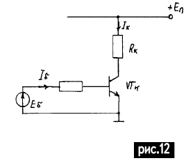
When using high powers in the load, for the normal operation of the converter, it is necessary to carry out special transistor switching modes. Let's consider two transient processes. The transition process of turning on an n-p-n transistor with OE, when a positive base current jump is set to its input (Fig. 12) [5].
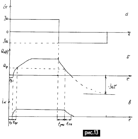
At the initial turn-on stage, the collector current is small, while the values of b are small, and the differential input resistance of the transistor is large. Therefore, we can assume that the base current goes to charge the input capacitance of the emitter, and at the same time the voltage at the emitter changes from zero to a certain value Ueo, corresponding to the on state of the transistor. For silicon transistors, Ueo = 0,7 V. The first turn-on stage has a delay time t3 (Fig. 13b). At the next stage - an increase in the collector current - the base current goes to the accumulation of charge carriers in the base. If there is a resistor Rk in the collector circuit during the transient process, the voltage at the collector junction changes, the barrier capacitance Sk is recharged, which increases the duration of the transient process (Fig. 13, c) tнр. When the transistor is operating in the key mode, an unlocking base current is supplied to its input, which is greater than the saturation current of the transistor Ibn = Ikn / β. This current corresponds to the boundary charge of electrons in the base Qgr = Ibn τ.
The process of turning off the transistor by a pulse of negative base current Ib = - Ib2. At the time t2 (Fig. 13, a), the base current abruptly decreases by the value ∆Ib = Ib1 + Ib2. The excess charge of holes in the base decreases for two reasons: due to the recombination of holes with electrons and the removal of holes from the base through the base electrode into the external circuit. In a similar way, the excess charge of minority carriers - electrons, is numerically equal to the charge of holes due to electrical neutrality. The change in the collector current begins after a certain time trac (the time of dissipation of the excess charge in the base). The resorption time increases with an increase in the opening current of the base Ib1 and decreases with an increase in the blocking current of the base Ib2. The stage of resorption is followed by the stage of formation of a negative front of the collector current, the duration of which is called the decay time tsp of the collector current and also decreases with an increase in Ib2. However, it should be borne in mind that even with forced on tnr and off tsp have a physical limit, i.e. these times cannot be less than the time of flight of electrons through the base. References:
Author: A.V.Kravchenko
Machine for thinning flowers in gardens
02.05.2024 Advanced Infrared Microscope
02.05.2024 Air trap for insects
01.05.2024
▪ Airport Self-Driving Wheelchairs ▪ Friction turns metal into liquid ▪ Clothes splattered from the spray
▪ section of the site Experiments in chemistry. Article selection ▪ article Sauna in the garden. Tips for the home master ▪ article What animals do German biologists study under the Angelina Jolie Project? Detailed answer ▪ article Dealing with leaded gasoline. Standard instruction on labor protection ▪ article Automated lighting control. Encyclopedia of radio electronics and electrical engineering ▪ article Coin and apple. Focus Secret
Comments on the article: Oleg The article is superb! I have never seen such detailed explanations. I will look for similar articles about other types of iip.
Home page | Library | Articles | Website map | Site Reviews
www.diagram.com.ua |


 Leave your comment on this article: