|
|


 Arabic
 Bengali
 Chinese
 English
 French
 German
 Hebrew
 Hindi
Hindi Italian
 Japanese
 Korean
 Malay
Malay Polish
 Portuguese
 Spanish
 Turkish
 Ukrainian
 Vietnamese
|
ENCYCLOPEDIA OF RADIO ELECTRONICS AND ELECTRICAL ENGINEERING On the calculation of steps on a field-effect transistor. Encyclopedia of radio electronics and electrical engineering
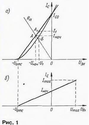
Encyclopedia of radio electronics and electrical engineering / Radio amateur designer calculating the steps of different steps on a field effect transistor will be much easier if you use a linear approximation of its characteristics, proposed by the author of this article. If the cutoff voltage and the initial drain current of a particular transistor instance are known, then such a step calculation gives a good agreement with practice. It is known that almost all literary sources describe the calculation of stages of amplifying stages with a field-effect transistor only in the mode of a small alternating current signal. It is not easy to find even recommendations for choosing the initial mode of the transistor. Meanwhile, for most practical cases, it is more necessary to calculate the steps for direct current. The technique proposed in the article makes it possible to calculate the steps of the most common nodes in practice - DC amplifiers, current stabilizers, etc. In this case, the calculation of the steps for alternating current in the small signal mode for low and medium frequency signals will be general calculation of steps for direct current. For definiteness, we confine ourselves to considering n-channel transistors with an integrated channel; for p-channels, you only need to change the polarity of the voltage. It is accepted that the transient characteristics lc=f(Uzi) of the transistor are approximated by a quadratic function. This is largely true for single channel transistors, but they have been out of production for a long time. At present, even low-power field-effect transistors are an assembly of several channels-cells connected in parallel, and powerful ones contain up to several hundred, sometimes thousands. Because of this and some other factors, the real transient response of such transistors lies between linear and quadratic functions. Approximation of a real characteristic by a quadratic function can only lead to a complication of the calculation of steps, which is not justified by the corresponding increase in accuracy. It is more expedient to use a linear approximation to calculate the steps. There are two characteristic points on the transient response of the transistor - the initial drain current Ico of the transistor, determined at Uzi = 0. and the so-called cutoff voltage Uotc (Fig. 1a). And if everything is clear with the first question, then with the second question it is more difficult.
The fact is that the transient characteristic asymptotically tends to the Uzi axis, which is why it is impossible to specify the voltage at which the drain current will be equal to 0 (i.e., the true cutoff voltage). Therefore, the conditional value U was adopted - the voltage at which the drain current is 10 μA, i.e., an easily measured value. However, it is precisely near this point that the characteristic has a particularly sharp bend, which gives the largest component of the error in the linear approximation. It would be more correct to determine the second point at the beginning of the section of the bend, for example, according to the criterion for reducing the differential value of the steepness or according to a certain value of the drain current. Unfortunately, the lack of reliable statistics on the transient characteristics of modern field-effect transistors does not allow us to clearly resolve this issue. Therefore, one has to accept a linear approximation with respect to two standard points - lco and Uotc. The accompanying error in most cases does not exceed 15%, which is quite sufficient for practice. On fig. 1, and the thick straight line shows a linear approximation of the real characteristics of the transistor. On fig. 2 shows a source follower circuit as an example. When Vin = 0 (if you close the input of the repeater to a common wire), the operating point A is at the intersection of the transient characteristic and the load line R and (Fig. 1). The real operating point is at the intersection of the actual transient response and the load line - this is point B. The figure illustrates the nature of the error due to linear approximation.
The initial position of the operating point A for the current Istart, determines the expression: Istart = Ico / (S·Ri+1). and in terms of voltage, it can be expressed as Unach Ri = lco Ri Rn/(S Ri+1). where S \u2d lco / Uotc is the average slope of the characteristic, and Ri is the resistance of the resistor Ri (Fig. XNUMX). When the gate is connected to a common wire, the repeater becomes a current-stabilizing two-terminal network (current stabilizer). According to the first formula, you can calculate the stabilization current. The minimum voltage at which the device enters the current stabilization mode is . The voltage drop across the transistor channel UCi is determined either by a family of output characteristics or experimentally. If Ri = 0. The stabilization current is maximum and equal to Iso, the output resistance is minimal and almost equal to the output resistance of the transistor. With the supply of a constant (for example, positive) voltage Uin to the input of the source follower, the operating point is shifted to position A, and its new current coordinate I corresponds to the expression: Ri+1). The value of the transistor closing voltage will be determined at It=0 - it is equal to Uotc. In terms of voltage, the new position of the operating point can be expressed by the relation: Ut=lt Ri=Ri(lco+ Uin. S)/(S Ri+1). The limits of the input voltage in the region of positive values are generally described by the formula: Uin = [Imax(S·Ri+1)-lco]/S, where Imax is the maximum current of the transistor. Maximum current Imax. limited by several factors. So. for transistors with a gate in the form of a p-n junction, it should not exceed Ic0, otherwise the gate will go into forward bias mode and the input resistance of the transistor will decrease sharply. With this in mind, the last formula is simplified: Uin = lCo·Ri. The boundary of the operating interval on the side of the negative voltage does not depend on the initial operating mode of the transistor and always starts from Uotc. It follows from the foregoing that in order to extend the operating interval, a transistor with a large Uotc value should be chosen. For an insulated gate transistor, the value is limited only by the current limit allowed for the device or the allowable power dissipation. In any case, 1max. cannot exceed Upit/Ri. When calculating the steps for a particular step, the value of I is determined by each of the factors discussed above, the smallest is chosen, and it is this that is substituted into the formulas. Transforming the expression for Ut, we obtain Ut = Ico Ri/(S Ri+1 )+Uin S Ri/ (S Ri+1). This formula clearly shows that the characteristic Uout = f(Uin,) for a streaming repeater is linear. The conversion steepness Kns of the source follower is equal to: Кns = ΔImax/ ΔUin = S/(S·Ri + 1). Accordingly, the voltage transfer coefficient Knu = Knl·Ri = S·Ri/(S·Ri+1). On fig. 1b shows the characteristic Ic = f(Uin) of the source follower. The transfer characteristic Uout = f(Uin) has a similar form. since Uout \uXNUMXd Ic·Ki. On fig. 3 shows a diagram of a typical amplifying stage, in which the transistor is assembled according to a common-source circuit with a resistor R and automatic bias.
The initial mode of the transistor is determined by the resistance of this resistor. When setting the current mode of the transistor (in the absence of an input signal), the resistance of the resistor can be determined by the formula: Rand \uXNUMXd (Iso "Inach) / Inach S. Usually, the operating point is chosen in the middle of the characteristic, i.e. Istart = Ico / 2 and Ustart = Uotc / 2, and this formula is simplified: R and = I / S = Uotc / Ico. If the initial position of the operating point on the characteristic should be asymmetric (for example, in the case of an asymmetric input signal), the resistance of the resistor R and at a given value of Uinit, the initial offset is determined by the formula: Ri = Uinit / (lco-Uinit S). The voltage at the drain of the transistor will be equal to Uc \uXNUMXd Upit - Inach ·Rc. With a symmetrical signal, the resistance of the resistor Rc, which provides the maximum range of the output voltage in the absence of distortion, is found by the formula: Rc \u2d (Upit - Unach) / 0.5I. If the operating point is chosen in the middle of the transfer characteristic of the transistor, then Rc = (Upit - XNUMXUotc)lco. Resistor R and is an element of the negative OS. reduction stage. To eliminate the action of the OS on alternating voltage, they usually include a blocking capacitor Cbl shown in Fig. 3 dashed lines. With this capacitor, the amplitude of the negative half-waves of the input signal should not exceed a value equal to the cutoff voltage of the transistor. It is also possible to eliminate the action of the OS on alternating voltage in another way - by including in the source circuit of a transistor instead of a resistor an element whose voltage depends little on the current flowing through it, for example, a direct-on diode, a stabistor, etc. However, such a circuit design solution is only possible in the case when the voltage on this element will be equal to Unach. If the voltage on the element is somewhat less, then an additional resistor of small resistance is connected in series with it. The transfer coefficient Knu of a stage assembled according to a common source circuit is determined by the well-known expression: Knu=S·Rc. If there is a resistor in the source circuit, Knu decreases: Knu=S·Rc/ (S·Ri+1)=lco·Rc/(lco·Ri+Uotc). The signal at the drain of the transistor VT1 (output 1) is in antiphase with the input, and the signal at the source (output 2) is in phase, which allows this stage to be used as a phase splitter. Usually, phase splitters are required that the signal amplitude values for both outputs be equal: Uout1 = Uout2 or lc·Rc=lи·Rи. Since lc=l and the condition for equality of amplitudes looks like this: Rc = Rand. In this case, the values of the transmission coefficient for both outputs will also be equal. Transfer coefficient, resistance of resistors Rc and Rand. as well as other necessary parameters can be calculated using the formulas presented above. Consider, for example, the conditions under which the stage according to the scheme in Fig. 3 turns on output 1 into a linear inverter with Knu = 1. Equating Knu in the last formula to one, we get Rc - Ri \u1d XNUMX / S \uXNUMXd Uotc / Ico. Such a stage, by analogy with a similar one on a bipolar transistor, can be called a drain follower. Author: A. Mezhlumyan, Moscow
Air trap for insects
01.05.2024 The threat of space debris to the Earth's magnetic field
01.05.2024 Solidification of bulk substances
30.04.2024
▪ Biodegradable plastic from cotton waste ▪ Samsung to launch 3GB mobile memory ▪ Portable supercomputer for unmanned vehicles ▪ Robots will be taught to more accurately follow the desired scenario ▪ The material of the future that becomes stronger under stress
▪ section of the site Winged words, phraseological units. Selection of articles ▪ article Rotary engine. History of invention and production ▪ article What do camels store in their humps? Detailed answer ▪ article Pedal scooter. Personal transport ▪ article High voltage transformer. Encyclopedia of radio electronics and electrical engineering ▪ article Four kings end up together. Focus Secret
Home page | Library | Articles | Website map | Site Reviews
www.diagram.com.ua |


 Leave your comment on this article: