|
|


 Arabic
 Bengali
 Chinese
 English
 French
 German
 Hebrew
 Hindi
Hindi Italian
 Japanese
 Korean
 Malay
Malay Polish
 Portuguese
 Spanish
 Turkish
 Ukrainian
 Vietnamese
|
ENCYCLOPEDIA OF RADIO ELECTRONICS AND ELECTRICAL ENGINEERING Switches for video and audio signals on microcircuits. Encyclopedia of radio electronics and electrical engineering
Encyclopedia of radio electronics and electrical engineering / Телевидение The ability to connect several external signal sources (VCR, video player, camcorder, video player, etc.) to modern TVs is a very important function. About the switches of video and audio signals on transistors, materials have already been published in our magazine. Here the author offers a description of designs on microcircuits that can be used in both new and old devices. A switch that allows you to connect external video and audio sources to the TV. - an obligatory component of any modern TV. In domestic equipment, such devices have been used since the second generation of color TVs. In receivers UPIMTST. for example, on the board of the signal processing unit (BOS) there is a place for installing the PA module 1-5. for pairing a VCR (VCR) with a TV. Such a module is installed on a connector plug (if not, then it is installed) with seven contacts. The module uses ten transistors. Its scheme is considered in [1]. The UM1-5 module operates in two modes: playback of programs from video cassettes and recording on-air programs on them. It has a two-wire input-output and is designed for operation with VCRs that also have common signal input-output jacks. This circumstance makes it difficult to use it with new VM models, which have separate inputs and outputs. Connecting the module to video players does not seem to present any difficulties. But the power supply of the module and its inclusion in the playback mode is provided only from the VM. and modern devices do not produce the necessary voltages, which does not allow the use of PA 1-5 without modification for communication with such video equipment. The ZUSST series TVs use the same UM 1-5 module, which has undergone a slight upgrade. Another transistor appeared in it, the connector for installing the module on the RTO board already has ten contacts. The schematic diagram of this version of the PA 1-5 module is published in [2]. The system of its power supply and control of operating modes has not changed, and the disadvantages have remained the same. The industry produced another version of this module under the same name. This model was different from the previous one, designed for ZUSCT TVs. topics. that it received power not from the VM, but from the TV. The control of the module still came from the VM. This model is used in the fourth generation TVs "Rubin - ТЦ4102/4103/4105". Its scheme is described in [3]. In TVs SELENA-CTV441, TVT441. GORIZONT-STU518 used a module for matching with external devices SUS-45. in which the previously mentioned shortcomings are eliminated. The module contains five transistors. For this purpose, the HORIZONT-CTV510 TV uses the MUS-501 module with five transistors and two microcircuits. Schematic diagrams of these two modules are considered in [4]. Similar devices for TVs of different designs, starting with ULPCT. offered on radio markets. Radio amateurs are also showing great interest in their creation. Many of them have developed such devices mainly on transistors and relays. The last version of such a switch was described in [5]. In televisions of the fifth and next generations, video and audio signal switches are already being implemented. usually integrated. They use specialized microcircuits, and in some cases (for example, in TVs based on TDA8360-TDA8362 microcircuits and their analogues), switches are included in the structure of the microcircuits themselves. The advantages of using microchips are obvious. They allow you to simplify the design of the signal switch, get rid of mechanical devices, improve the decoupling of inputs and outputs. Today, radio amateurs have many microcircuits at their disposal that can switch signals from any number of sources. Their supply voltage is different and usually ranges from 5 to 15 V. Consider those of them. which are powered by 12 V. available in all domestic TVs. In ZUSTST devices, the simplest option for switching video and audio signals for two sources (for example, from a TV radio channel and from a VM) can be a device built on a TEA1014 chip from SGS-THOMSON. Its scheme is shown in Fig. 1. Chip DA1 has three electronic switches that switch video (S1) and audio (S2) signals. Switch S3 in the AV position connects pin 7 of the HZ connector (A1) - change t APCIF - with a common wire.
Video and audio signals from the radio channel module (RCM) of the TV through pins 1 and 5 of the XZ connector (A1) pass to pins 3 and 8 of the DA1 chip. The same signals from an external source are sent to pins 14 and 7 of the microcircuit. From pins 12 and 6, video and audio signals come to pins 4 and 2 of the XZ connector (A1), and from them to the RTO. Switch the signal sources with the SA1 toggle switch. To turn on the on-air program (TV), you need to apply +12 V to pin 10 of the microcircuit and connect pin 11 to a common wire. To turn on an external source (AV), a voltage of 12 V is applied to pin 11 and pin 10 is connected to a common wire. When switching to the AV mode, it is necessary to ensure that the line-scan APCF device switches to the operating mode with a wide capture bandwidth. This is achieved by connecting pin 7 of the XZ connector (A 1) with a common wire inside the microcircuit, when its output 10 is connected to a common wire when the SA1 toggle switch is set to the "AV" position. The purpose of the pins of the plug and socket of the XZ connector (A1) in fig. 1 is specified differently. On the plug, it corresponds to the factory MRK scheme. considered in [2]. and on the socket - to the purpose of the circuits in the switch. The switch board is connected to the XZ connector plug on the MRK radio channel board, intended for the UM 1-5 module. If there is no such plug, then it should be installed in the sockets provided for it. When using the switch in the MRK of the ZUSTST TV, it is necessary to make the changes shown in fig. 1: remove the chain sections shown with dashed lines and lay new chains drawn with thick lines. The essence of the modification is as follows. According to the MRK factory circuit, the video signal from output 7 of the SMRK-2 submodule passes in parallel to pin 1 of the X1 connector, to the USR unit through pin 8 of the X1.4 connector (A 1) and to the color module through pin 6 of the X2 connector (A2). According to the new scheme, the connection of SMRK-8 and the XZ connector is retained, and the signal arrives at the X1.4 (A6) and X2 (A4) connectors after switching in the switch through pin XNUMX of the XZ connector. The audio signal from pin 23 of SMRK-2 came to resistor R6. Now it should pass into the switch to pin 5 of the X1 connector (A 6), and the resistor R2 needs to be signaled from the switch output (pin XNUMX of the XXNUMX connector). When using the UM 1-5 module in the playback mode of the VM signals, a command to block the UPCH and UPCHZ is sent to the TV from the module. Changing the transmission chains of video and audio signals eliminates such blocking and allows you to constantly feed the on-air program from the TV to the VCR. Therefore, pin 6 of the X1 connector (AXNUMX) is left free. Switch for two sources, the appearance of which is shown in fig. 2, assembled on a board made of double-sided foil fiberglass with a thickness of 1,5 mm. Its drawing and placement of parts on it are shown in Fig. 3. Printed conductors from pin 7 of the XZ connector (A1) to pin 5 of the DA1 chip and or capacitor C6 to its pin 8 are drawn on the board from the side of the parts (shown by dashed green lines). The arrows on the X21 connector are metal stops that are set to ensure proper connection.
Resistors R1 and R2 are chip components of size 1206 or 0805, the rest are MLT with a tolerance of ± 10%. Capacitor C11 - K50-35 or any oxide small-sized. C1. C3. Sat. C7. C10 - tantalum of any type, the rest - K10-17. X1 connector (A21) - socket with ten pins, XXNUMX - socket with six pins. On fig. 4 shows a schematic diagram of a signal switch for three sources: TV, AV1, AV2, where AV1 is a VCR with separate inputs and outputs, and AV2 is a video device that does not have a signal recording function (video player, game console, laser disc player).
The switch is assembled on two TOSHIBA TA7348P microcircuits designed to switch both video and audio signals. Its scheme has no fundamental differences from that shown in Fig. 1, and it requires the same modifications in the MRK TV. Only the control circuits and signal generation "Change t APCiF" have been changed. To switch signal sources, two toggle switches are used: SA1 with the positions "TV" and "AV and SA2 with the positions MAV1" and "AV2". The signal "Change t APCHIF" (it must be equal to 0 V in the modes AV1, AV2) is fed to pin 7 of the X1 (A1) connector from pin 21 of the XXNUMX connector. Switch for three sources, the appearance of which is shown in fig. 5 are assembled on the same board as described above.
A drawing of a printed circuit board and the placement of parts on it are shown in fig. 6.
Resistors R1, R3 are chip components, the rest are MLT with a tolerance of ± 10%. Capacitor C12 - oxide. C2, C7-C10 - tantalum. the rest - K10-17. The switches use chip components, so far rarely used in amateur radio practice. These are resistors, capacitors, coils, diodes and transistors in miniature design. Chip resistors and capacitors are made in the form of rectangular cases of standard sizes. Cases have digital designations: 0603, 0805,1206,1210,1808, etc. The first two digits indicate the length of the case in hundredths of an inch, the last - its width. The 1206 and 0805 packages are the most common and easy to mount. The chip resistor in the 1206 package is 0,12 inches (3,2 mm) long and 0,06 inches (1,6 mm) wide with a height of about 1 mm. Chip components come from the manufacturer packaged in individual cells of paper tape and must be stored in this package until installation. More detailed information about the features of their installation, verification and dismantling can be found in [6]. Chip components are mounted on sites with dimensions shown in Fig. 7. In fractional sizes, the numerator means the size for the case 1206, the denominator - for the 0805. All dimensions are in millimeters.
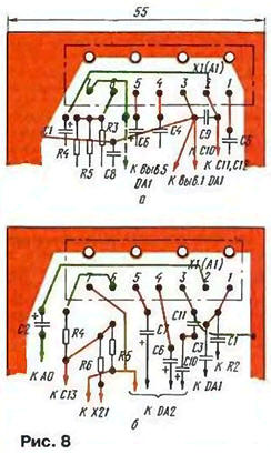
It is recommended to mount the chips in the following order. Mounting pads (tinned) are covered with solder paste and a chip is applied to them. Due to the viscosity of the paste, this almost weightless body is fixed in the right place during the soldering process. Then the chip is placed more precisely and fixed for the time of soldering with a narrow screwdriver, a wooden stick. Interestingly, the chip resistor, unlike other chip parts, is attracted to a metal screwdriver, which is usually magnetized. The ends of the chip body are metallized with nickel and tin (or solder) on top. Metallization captures narrow strips on the upper and lower parts of the case at the ends. Solder the chip. using solder POS-61. The power of a soldering iron with a sharp tip should be no more than 30 watts. Due to the small distance between the mounting pads and their proximity to the adjacent printing lines, undesirable jumpers may appear. Their absence is checked with an ohmmeter. When working with chips, it is recommended to use a magnifying glass. It should be borne in mind the characteristic feature of the chip components. During installation, due to air vibrations, they can "fly away" at any time. Therefore, special care must be taken when removing them from the package, putting them back in place, at the beginning of soldering, etc. If you want to have a switch for four or five video inputs, you should also use the appropriate microcircuits: for example. BA7644AN. ROHM's BA7649A can switch four inputs, while ROHM's BA7649A can switch five. To switch the audio inputs, you need two TA7348P chips connected in series. Three signal sources are connected to the inputs of one of them, and the output of the first microcircuit and other sources are connected to the inputs of the other. The control of their switching will, of course, become more complicated, but the circuit is easy to implement, taking into account the options considered in Fig. 1 and 4 in the first part of the article. The outer frame (attachment parts) of the microcircuits and the method of generating the signal "Change τ APCiF" can be similar to the option for three sources (see Fig. 4), adjusted for a different pinout of the microcircuits. Their block diagrams and pinouts are available in [7]. Switches, the schemes of which are shown in fig. 1 and 4. can be used in UPIMTST TVs. They (as already mentioned) install a seven-pin version of the UM 1-5 module. To connect the considered switches, the XZ socket (A1) must also have seven contacts in them, which requires changes to the printed circuit boards. They are shown in fig. 8,a - for the first version of the switch and in fig. 8b - for the second. Circuits that are not modified are shown in red, new ones in green.
Changes on the BOS board required when using any switch option are shown in fig. 9.
All of the above applies to TVs with push-button devices for selecting programs USU-1-15 and SVP (KVP. MVP) of any type. Switching between operating modes and signal sources in them is provided by toggle switches installed on the front panel of the TV or in any other convenient place. If the voltage synthesizer MSN-405 (or MSN-501) is installed on the TV, then you can control the signal switch through it. Switch control according to the diagram in fig. 1 is provided by the AV / TV signal generated at pin 12 of connector X2 (A1) of the MCH-405 synthesizer (or at pin 8 of connector X7 (A1) in MCH-501). In the MCH-405, it occurs when you press the VCR buttons on the remote control or the keyboard on the front of the TV. In MSN-501, press the AV or TV buttons on the remote control. To implement this control method in the switch according to the diagram in Fig. 1 needs to be modified according to Fig. 10.
Toggle switch SA1, resistors R4 and R5 are not needed. A transistor VT1 and resistors R21 are additionally installed on the board in a free place. R22. In the case of using the MSN-405 synthesizer, it will also be necessary to achieve the required voltage level at pin 32 of the microcontroller, guided by the instructions in section i8AA1293A and the reference book [8]. If a three-source signal switch is used, then two signals are required to control it: AV / TV and AV1 / AV2. In MCH-501, the first of them, as already mentioned, is removed from pin 8 of connector X7 (A1) of the synthesizer, and as the second one, the switching signal for PAL or SECAM broadcasting standards is suitable - pins 12 or 15 of connector X10 (A1 of the synthesizer. This signal when installing the MSN-501 unit in a TV set, the ZUSTST is not needed, and the outputs remain free.The AV / TV signal is generated by pressing the AV and TV buttons on the remote control. The AV1 / AV2 signal is generated by pressing the SS button on the keyboard of the synthesizer. shown in Fig. 11, a. Toggle switches SA1, SA2, resistors R5 and R6 and diode VD1 are not needed.
Note that there are several modifications of such a synthesizer produced by various enterprises. They have some differences. So, in the MCH-503 synthesizer (similar to the MCH-501) and some models of the MCH-501, the SS button (switching standards) is replaced by the CL button (memory clear). In this case, to generate the AV1 / AV2 signal, you will have to install a toggle switch. In some MCH-501 models, PAL, SECAM signals from the microcontroller pins do not come to the X10 (A1) connector. To eliminate this shortcoming, you need to connect pin 38 of the microcontroller DD2 with pin 15 of connector X10 (A 1) through the circuit shown in fig. 11b. As for the MSN-405 synthesizer, the SAA1293A microcontroller used in it has pin 25, on which a color standard selection signal is generated. However, it is impossible to use it, since there are no buttons for controlling this function on the remote control and keyboard of the synthesizer. You have to use an external toggle switch to switch AV1 / AV2. All microcircuits indicated in the article are available in the catalogs of trading companies at a price of 0.4 to 1 USD. The switch, assembled from tested parts, does not require adjustment, and after checking for a short circuit in the +12 V supply circuits, it can be installed on a TV. The performance is checked by switching the toggle switches (remote control buttons and keyboard). You should also make sure that in the TV mode, a voltage of 7 ... 1 V is supplied to pin 5 of the X11 connector (A12), and in the AV mode it is equal to zero. The current consumption in the 35V circuit is about 1 mA for the switch according to the diagram in fig. 27 and about 4 mA - at the switch according to the diagram in fig. XNUMX. Literature
Author: V.Brylov, Moscow
Alcohol content of warm beer
07.05.2024 Major risk factor for gambling addiction
07.05.2024 Traffic noise delays the growth of chicks
06.05.2024
▪ Brain implant and prosthesis restore sense of touch to paralyzed man ▪ Does a foreign language help you think?
▪ section of the site Amateur radio calculations. Article selection ▪ article Give the world a chance. Popular expression ▪ Why don't dogs recognize themselves in the mirror? Detailed answer ▪ article Vice-rector for academic work of a higher educational institution. Job description ▪ Article Means for simultaneous bleaching and washing. Simple recipes and tips ▪ article AM broadcast receiver. Encyclopedia of radio electronics and electrical engineering
Home page | Library | Articles | Website map | Site Reviews
www.diagram.com.ua |


 Leave your comment on this article: