Transceiver input circuit. Encyclopedia of radio electronics and electrical engineering

Encyclopedia of radio electronics and electrical engineering / Nodes of amateur radio equipment
 Comments on the article
The authors of all transceiver designs have to deal with the problem of antenna switching between the receiving and transmitting paths. The use of electromagnetic relays for these purposes reduces the reliability of the device as a whole and limits the upper speed limit for half-duplex telegraph operation. High reliability and speed have electronic switching circuits. Many tube output stage designs use a circuit similar to that shown in Figure 1. C1, L1, C2 form a P-circuit, the coupling capacitor Ccv has a capacitance of 1 ... 5 pF, the L2C3 circuit has a high quality factor and is used as a narrow-band preselector during reception. Diodes VD1, VD2 are used to protect the UHF from the powerful signal of its transmitter.
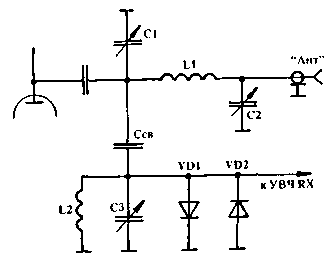
Ris.1
The circuit is simple and reliable in operation, however, as the experience of its operation on my radio station has shown, often in the ranges of 15 and 40 meters, when trying to fine-tune the L2C3 preselector circuit to the frequency of the received station, the air is clogged with all sorts of interfering signals and interference. This happens due to the conversion of powerful signals from broadcasting stations nearby in frequency ranges of 16 and 41 m, respectively, on the non-linear resistance of the diodes VD1, VD2. You can get rid of this disadvantage by simply reducing Cc, but this leads to a loss of sensitivity. A fairly effective measure of struggle is to apply a blocking bias to the diodes in the RX mode, but this does not completely solve the problem. I managed to completely get rid of this drawback by assembling the input circuit according to the scheme of Fig. 2.
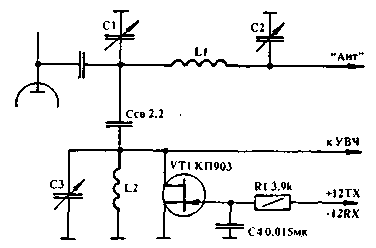
Ris.2
Range switching circuits are not shown in the figure. The transistor is controlled by applying a voltage of the appropriate polarity to the gate. Resistor R1 limits the forward biased gate current to a safe level, its value is not critical. With a negative gate voltage, the resistance of the VT1 channel is very high, and it does not worsen the quality factor of the L2C3 preselector circuit.
An important advantage of a field-effect transistor is the linearity of the channel resistance at low drain-source voltages, therefore, no frequency conversions occur on it. In transmit mode, a positive bias reduces the channel impedance to a few ohms, which shunts the UHF RX input and protects it from the transmitter signal. Control voltages may be different. For this type of transistor, the control voltage of the RX mode can be within (-10 ... -15V), the TX mode - 0 ... 15V.
Author: V. Vishnevsky (UB5AJS), Sumy. Publication: N. Bolshakov, rf.atnn.ru
 See other articles Section Nodes of amateur radio equipment.
Read and write useful comments on this article.
<< Back
 Latest news of science and technology, new electronics:
Artificial leather for touch emulation
15.04.2024
In a modern technology world where distance is becoming increasingly commonplace, maintaining connection and a sense of closeness is important. Recent developments in artificial skin by German scientists from Saarland University represent a new era in virtual interactions. German researchers from Saarland University have developed ultra-thin films that can transmit the sensation of touch over a distance. This cutting-edge technology provides new opportunities for virtual communication, especially for those who find themselves far from their loved ones. The ultra-thin films developed by the researchers, just 50 micrometers thick, can be integrated into textiles and worn like a second skin. These films act as sensors that recognize tactile signals from mom or dad, and as actuators that transmit these movements to the baby. Parents' touch to the fabric activates sensors that react to pressure and deform the ultra-thin film. This ... >>
Petgugu Global cat litter
15.04.2024
Taking care of pets can often be a challenge, especially when it comes to keeping your home clean. A new interesting solution from the Petgugu Global startup has been presented, which will make life easier for cat owners and help them keep their home perfectly clean and tidy. Startup Petgugu Global has unveiled a unique cat toilet that can automatically flush feces, keeping your home clean and fresh. This innovative device is equipped with various smart sensors that monitor your pet's toilet activity and activate to automatically clean after use. The device connects to the sewer system and ensures efficient waste removal without the need for intervention from the owner. Additionally, the toilet has a large flushable storage capacity, making it ideal for multi-cat households. The Petgugu cat litter bowl is designed for use with water-soluble litters and offers a range of additional ... >>
The attractiveness of caring men
14.04.2024
The stereotype that women prefer "bad boys" has long been widespread. However, recent research conducted by British scientists from Monash University offers a new perspective on this issue. They looked at how women responded to men's emotional responsibility and willingness to help others. The study's findings could change our understanding of what makes men attractive to women. A study conducted by scientists from Monash University leads to new findings about men's attractiveness to women. In the experiment, women were shown photographs of men with brief stories about their behavior in various situations, including their reaction to an encounter with a homeless person. Some of the men ignored the homeless man, while others helped him, such as buying him food. A study found that men who showed empathy and kindness were more attractive to women compared to men who showed empathy and kindness. ... >>
| Random news from the Archive Tunnel under the Yangtze
07.12.2007
For the next World Expo due to open in Shanghai in 2010, a double road tunnel 9 kilometers long and over 15 meters in diameter is being built under the mouth of the Yangtze.
There are two German tunneling shields with a diameter of 15,43 meters - the largest in the world. In a relatively soft soil from river sediments (silt, sand and clay), the shields pass 400 meters per month.
The rapid development of the road network in China required the construction of many tunnels. In 2006, the country purchased from different manufacturers, mostly German, more than fifty tunneling shields.
|
Other interesting news:
▪ New generation rover
▪ Discovery of waves in Jupiter's magnetosphere
▪ Everyone lives in their own reality
▪ Microsoft experimental underwater data centers
▪ Corn has a brain
News feed of science and technology, new electronics
 Interesting materials of the Free Technical Library:
▪ Telephony site section. Article selection
▪ article Damaging factors of a nuclear explosion. Basics of safe life
▪ article Why does a comet have a tail? Detailed answer
▪ article Cinchona reddish. Legends, cultivation, methods of application
▪ Article Toothpaste. Simple recipes and tips
▪ article Light Probe. Encyclopedia of radio electronics and electrical engineering
Leave your comment on this article:
 All languages of this page
Home page | Library | Articles | Website map | Site Reviews

www.diagram.com.ua
2000-2024


 Arabic
 Bengali
 Chinese
 English
 French
 German
 Hebrew
 Hindi
Hindi Italian
 Japanese
 Korean
 Malay
Malay Polish
 Portuguese
 Spanish
 Turkish
 Ukrainian
 Vietnamese