|
|


 Arabic
 Bengali
 Chinese
 English
 French
 German
 Hebrew
 Hindi
Hindi Italian
 Japanese
 Korean
 Malay
Malay Polish
 Portuguese
 Spanish
 Turkish
 Ukrainian
 Vietnamese
|
ENCYCLOPEDIA OF RADIO ELECTRONICS AND ELECTRICAL ENGINEERING IF amplifier based on PBS. Encyclopedia of radio electronics and electrical engineering
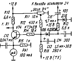
Encyclopedia of radio electronics and electrical engineering / Nodes of amateur radio equipment On fig. 1 shows a schematic diagram of a 500 kHz IF amplifier based on the so-called series-balanced transistor structure (STS). The gain of the device is about 6000 (62 dB). Despite this, the amplifier is resistant to self-excitation and has good dynamic characteristics. A small number of parts and a small current consumption allow it to be used in small-sized portable radio stations.
The amplifier is assembled on transistors VT1-VT3, galvanically connected to each other. The quiescent current of all three transistors is set automatically and depends on the resistance of the resistor R3. Any changes in the mode of one of the transistors (for example, during temperature fluctuations) immediately lead to a change in the mode of the others, and the quiescent current returns to its previous value. As you can see, a parallel oscillatory circuit L1C2 is included at the input of the amplifier, and a series circuit L3C3 is connected to the VT7 emitter circuit. The load is a ring balanced mixer on diodes VD1-VD4. Matching the input impedance of the latter with the output impedance of the amplifier is carried out by the transformer T1. The R5C5 circuit protects the device from interference in the power circuit.
If necessary, it is not difficult to introduce gain control into the device, using, for example, the circuit shown in Fig. 2 (the numbering of parts on it and subsequent figures continues what was started in Fig. 1). In this case, the upper (according to the diagram) output of the resistor R1 is disconnected from the power circuit and connected to the collector of the transistor VT4. The gain is regulated by a variable resistor R11. Microammeter RA1 is used as an S-meter. When a +2 V voltage is applied to the lower (according to Fig. 16) output of the resistor R12, the amplifier closes (the gain tends to zero). The need for this arises during transmission when using it in a transceiver. Coils L1-L3 are wound in bulk on plastic frames with a diameter of 5 mm with trimmers made of carbonyl iron from armored magnetic cores SB-9a. For an IF equal to 500 kHz, coils L1 and L3 should each contain 70 turns of PEL 0,24 wire, and L2 - 20 turns of the same wire wound over L1. As the magnetic circuit of the RF transformer T1, a ferrite (600NN) ring magnetic circuit of the size K10x6x4 is used. Its windings I (45 turns) and II (15 turns) are wound with PELSHO 0,24 wire. The amplifier is tuned in the absence of an input signal by selecting the resistor R3 until the emitter current of the transistor VT1 is equal to 0,5 mA. Then, a signal with a frequency of 501 kHz is applied to the input and, by changing the inductance of the coils L1 and L3 by moving the trimmers, a maximum 3-hour signal is achieved at the output. The amplifier can also be used for other IF values. So, with an IF equal to 5 MHz, coils L1, L3 and L2 should contain, respectively, 31, 31 and 5 turns of wire PEL 0,24, windings I and II of the transformer T1 - 15 and 5 turns PELSHO 0,24. The capacitance of capacitors C2, C7 in this case should be equal to 100, C4 - 1200 pF, and C3-0,015 μF.
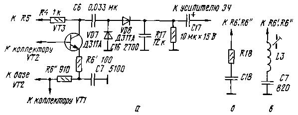
On fig. 3a shows the connection diagram of the amplitude detector to the described amplifier. With an IF of 500 kHz, the values of capacitors C7 and C 16 should be respectively equal to 5100 and 2700, with an IF of 5 MHz - 1200 and 270 pF. To obtain the required frequency response, instead of capacitor C7, series circuits R18C18 (Fig. 3, b) and L3C7 (Fig. 3, c) are used. By selecting the parameters of the elements included in them, it is possible to change the resonant characteristic of the amplifier over a wide range. The bandwidth (and at the same time the gain) is regulated by the selection of resistor R6. In this case, the total resistance of resistors R6' and R6 must remain equal to 1 kOhm. When replacing the L3C7 circuit with a 0,033 uF capacitor and excluding L1 C2, the amplifier becomes broadband with a slight rise in the frequency response in the 500 kHz region. When replacing C4 and the L3C7 circuit with 1200 pF capacitors, a slight rise in the frequency response is observed in the 5 MHz region.
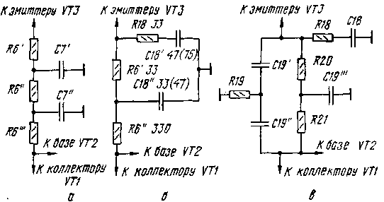
To obtain other characteristics, instead of the resistor R6 (and, if necessary, R2), you can use circuits, the diagrams of which are shown in Fig. 4. For example, the circuit according to the diagram in fig. 4,6 will help form a two-hump characteristic with a slight dip in the middle. To do this, one such circuit (with the values \u18b\u18bof capacitors C2 'and C6 "indicated outside the brackets) is included instead of R4, and the other (with the values \u3b\u7bspecified in brackets) instead of R25 and at the same time excludes elements C40, L100 and C120. The bandwidth of the amplifier with such refinement - XNUMX ... XNUMX MHz By changing the values of the elements of the introduced circuits, the "resonant" characteristic of the amplifier can be shifted in the frequency band from XNUMX kHz to XNUMX MHz. When using a circuit made according to the scheme in fig. 4, c, the frequency response of the amplifier is determined by the quasi-resonance frequency of the double T-shaped bridge R19C19C19 "R20R21C19" '. Quasi-resonance frequency f is calculated by the formula: f = 1/2pRC, where R is the resistance of resistors R20, R21 (1 kOhm); R19=0,5R=510 Ohm; C - capacitance of capacitors C19, C19", C19 "=2C. The R18C18 circuit plays the role of an additional selective element that corrects the overall frequency response of the amplifier. With an appropriate selection of elements of the corrective circuits, the amplifier is capable of operating in a wide frequency range - from several tens of kilohertz to 150 MHz (naturally, when using appropriate transistors). The bandwidth when using LC circuits is from 10 kHz (minimum value), when using RC circuits - up to 100 MHz (maximum value). It should be noted that when capacitors C4, C7 are excluded from the amplifier, a side quasi-resonance is observed in the frequency range of 200 ... 500 MHz due to the influence of parasitic capacitances. Author: Vladimir Rubtsov (UN7BV); Publication: N. Bolshakov, rf.atnn.ru
Artificial leather for touch emulation
15.04.2024 Petgugu Global cat litter
15.04.2024 The attractiveness of caring men
14.04.2024
▪ Listening to birdsong can reduce anxiety and depression ▪ Implanted electronic chips instead of regular passwords ▪ NASA will build a supersonic aircraft
▪ section of the site Electricity for beginners. Article selection ▪ article Wait for the weather by the sea. Popular expression ▪ article What is a warm front? Detailed answer ▪ article Heart-shaped linden. Legends, cultivation, methods of application ▪ article Predictive cards. Focus Secret
Home page | Library | Articles | Website map | Site Reviews
www.diagram.com.ua |


 Leave your comment on this article: