|
|


 Arabic
 Bengali
 Chinese
 English
 French
 German
 Hebrew
 Hindi
Hindi Italian
 Japanese
 Korean
 Malay
Malay Polish
 Portuguese
 Spanish
 Turkish
 Ukrainian
 Vietnamese
|
ENCYCLOPEDIA OF RADIO ELECTRONICS AND ELECTRICAL ENGINEERING Ultrasonic flaw detector. Encyclopedia of radio electronics and electrical engineering
Encyclopedia of radio electronics and electrical engineering / Indicators, detectors, metal detectors The flaw detector is designed to detect internal defects in welds (pores, cracks, non-fusion, slag inclusions, etc.) in metals and some plastics. The device allows you to determine at what depth the defect is within 7 ... 50 mm with an accuracy of ± 1 mm. The operating frequency of the flaw detector is 2,5 MHz. The operating mode setting time after power on is 0,5 s. Current consumption - 30 mA. The time of continuous operation of the flaw detector from nine batteries D-0,06-1,5 hours. Dimensions - 94X58X18 mm, weight - 205 g. The operating principle of the flaw detector is based on the property of ultrasonic vibrations (UK) to be reflected from internal defects of the material that conducts these vibrations. A short radio pulse is converted by the piezoplates В1-ВЗ of the detector (Fig. 1) into an ultrasonic pulse, which propagate through the layer of the contacting liquid in the material in the form of a divergent beam of transverse waves. The ultrasonic vibrations reflected from the defect, in turn, act on the V1-VXNUMX piezoelectric plates, excitation in them of the EMF, which is amplified, converted and fed to the defect detector. To eliminate false signals (reflections from the reinforcement bead, etc.), the presence of defects is determined by the signaling device only in the volume of weld fusion - the "control zone".
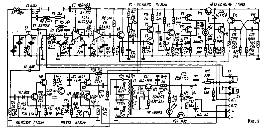
The flaw detector has two operating modes: "Search" and "Evaluation". Directional diagram width (Fig. 1) in the vertical plane in the "Search" mode - φ1=13°, and in the "Evaluation" mode - φ2=8,5°. This allows you to first determine the presence of a defect, and then its location. The entry angle (pho) depends on the welded materials, for steel it is 67°. The schematic diagram of the flaw detector is shown in fig. 2, and the timing diagram of its operation is shown in Fig. 3.
The flaw detector consists of a radio pulse generator, a defect detector, a broadband amplifier, a temporary amplitude equalization device, a supply voltage stabilizer and a converter. The radio pulse generator is assembled on a V1 dinistor. A current pulse passing through the V1 dinistor excites a radio pulse in the L1B3 circuit in the "Search" mode or L1B1-B3R1 in the "Evaluation" mode. Its duration at level 0,5 is 0,4 µs. The sensitivity of the device in the "Evaluation" mode is set by the resistor R43. The radio pulse taken from the part of the coil L1 is converted by the diode V2 into a positive pulse 1 (Fig. 3), which triggers the delay single vibrator of the defect detector on transistors V18, V19. The duration of the single vibrator pulse depends on the position of the slider of the resistor R30. The differentiated pulse 2 (Fig. 3) of the single vibrator, which passed through the inverter on the transistor V20, turns on the single vibrator of the "control zone" of the signaling device on transistors V22, V23. The pulse duration 3 (Fig. 3) of this single vibrator is regulated by the resistor R35 "P" (distance to the defect). From the collector of transistor V22, the pulse enters the base of transistor V6 of the coincidence device on transistors V6, V7 of the signaling device.
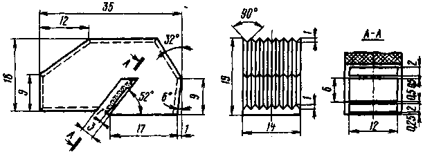
If a defect occurs in the "control zone", the pulse reflected from it and converted by the piezoelectric plates V1-VZ is amplified by a broadband amplifier on A1 microcircuits. A2. To protect the amplifier from overvoltages at the input, a two-way limiter is included on diodes V3, V4. Next, the radio pulse is detected and limited in the cascade on the transistor V5 of the defect detector and acts on the base of the transistor V7 of the coincidence device (pulse 4 in Fig. 3). Resistor R12 can change the pulse limit threshold in the detector-limiter. From the collector of transistor V8, a positive pulse first triggers a single vibrator of light (transistors V9, VIO), and then a single vibrator of sound (V12, V13) indicators, signaling the presence of a defect in the "control zone". The sound indicator, in addition to the single vibrator-pulse expander, contains a multivibrator on transistors V15, V16. If there is a defect, the LED H1 "D" (defect) lights up for a short time and a signal sounds in the telephones B4. To equalize the sensitivity of the device according to the depth of the defects, a device for temporal equalization of the amplitude of radio pulses on the R3R4C3 elements was introduced into the flaw detector. It generates pulses of negative exponentially increasing voltage, which are fed to the input of the chip A1, The stabilizer on the transistor V29 and the converter on the transistor V26 and diodes V24, V25 provide the flaw detector with the necessary supply voltages. Connector X1 is used to connect an external detector and power supply, as well as automated and semi-automated installations when operating a flaw detector as a set with them. In the flaw detector, capacitors C22 and C26 must have a small TKE. Transformer T1 is wound on a ring core made of M1500NM ferrite, size K16X8X6. Winding I contains 14 turns of wire PEV-1 0,6, winding II - 13 turns of wire PEV-1 0,12, windings III and IV - 350 turns of wire PEV.1 0,08 each. Coil L1 is wound on a mandrel with a diameter of 5 and a length of 3 mm and contains 40 turns of PELSHO 0,35 wire, the tap is made from the 8th turn, counting from the output connected to the common wire. The flaw detector finder (Fig. 4) is made of organic glass. The piezoplates are made of barium titanate, their dimensions are shown in the figure. Pre-fitted in size, and therefore in frequency, the plates are glued into the slots with epoxy glue.
The variable resistor R35 is made from the SP5-3 resistor. Its upper part is cut off with a file, the adjusting screw is removed, and a dial with a scale is attached to the slider with epoxy glue. The establishment of a flaw detector begins with the installation of stable generation in the voltage converter, selecting the resistor R39. Next, the required repetition rate (120 ... 150 pulses / s) of the radio pulse generator pulses is obtained by selecting the resistor R2. Amplitudes of radio pulses of 70 ... 80 V are achieved by selecting a dinistor V1. After that, by selecting capacitors C22 and C26, the limits of change during the rotation of the engines of resistors R30 and R35 are set for the duration of the pulses of the delay single vibrators (10 ... 25 μs) and the "control zone" (7 ... 45 μs). Then, placing the flaw detector on a sample of steel or organic glass with a defect in the form of a hole with a diameter of 2,5 ... 3 mm and a depth of 10 ... 50 mm, drilled perpendicular to the axis of the ultrasonic beam, the presence of a pulse reflected from the defect is checked at the control point KT1 . The amplitude of 1,8 ... 2 V of the pulse reflected from the defect is set alternately by resistors R43 and R12. Next, the slider of the resistor R4 is rotated until the amplitudes of the reflected signals from the same defects (holes) at different depths within 7 ... 50 mm do not differ by more than 20%. When working with a flaw detector, first lubricate the surface near the seam with a contacting liquid (water, oil or glycerin). Then set the disk "P" of the resistor R35 to the maximum distance and, by turning on the flaw detector with the S2 button in the "Search" mode, move it along the seam. The appearance of a sound signal in the phone indicates the presence of a defect in the "control zone". To determine the location of the defect, simultaneously press the buttons S1 "Estimate S2" and, moving the flaw detector across the seam, point the positions at which the light indicator W "D" goes out. Next, the flaw detector is installed in the middle between the found positions. , the scale determines the depth of the defect by the moment when the light indicator H "D" goes out. Authors: A. Bondarenko, N. Bondarenko; Publication: N. Bolshakov, rf.atnn.ru
Machine for thinning flowers in gardens
02.05.2024 Advanced Infrared Microscope
02.05.2024 Air trap for insects
01.05.2024
▪ LTC5508 Subminiature Broadband Power Detector ▪ Miniature chipset for mobile cameras ▪ Superfood that replaces meat ▪ The robot will find water on the moon
▪ site section Chargers, accumulators, batteries. Article selection ▪ article Extreme emergency situations in railway transport. Basics of safe life ▪ article How big can tortoises get? Detailed answer ▪ article Electrician of a traction substation. Standard instruction on labor protection ▪ article The wand is getting longer. Focus Secret
Home page | Library | Articles | Website map | Site Reviews
www.diagram.com.ua |


 Leave your comment on this article: