|
|


 Arabic
 Bengali
 Chinese
 English
 French
 German
 Hebrew
 Hindi
Hindi Italian
 Japanese
 Korean
 Malay
Malay Polish
 Portuguese
 Spanish
 Turkish
 Ukrainian
 Vietnamese
|
ENCYCLOPEDIA OF RADIO ELECTRONICS AND ELECTRICAL ENGINEERING Fundamentals of the theory of frequency synthesizers. Encyclopedia of radio electronics and electrical engineering
Encyclopedia of radio electronics and electrical engineering / Frequency synthesizers Introduction The phase-locked loop (PLL) is a widely used original node, which is produced by some companies as a separate IC. The PLL contains a phase detector, an amplifier and a voltage controlled oscillator (VCO) and is a combination of analog and digital technology. We will briefly look at the applications of PLLs for tone decoding, AM and FM demodulation, frequency multiplication, frequency synthesis, signal clocking under noisy conditions (such as magnetic recording), and signal recovery. There is a traditional anti-PLL bias that is partly due to the difficulty of implementing a PLL on discrete components, and partly based on the belief that a PLL cannot work reliably enough. However, the current advent of a large number of inexpensive and easy-to-use PLL devices quickly removes the first obstacle to their widespread use. If the PLL is properly designed and used to its limits, it is as reliable a circuit element as an op-amp or flip-flop.
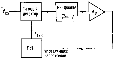
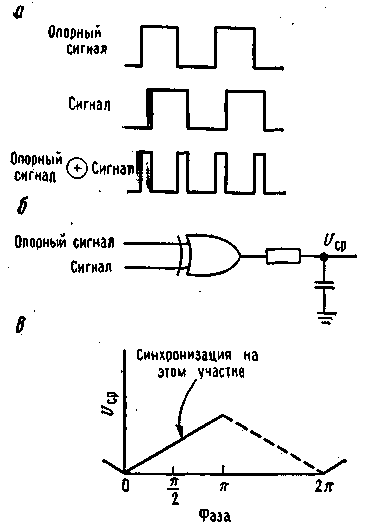
The classic PLL circuit is shown in Fig.1. The phase detector compares the frequencies of the two input signals and generates an output signal that is a measure of their phase mismatch (if, for example, they differ in frequency, then a periodic difference frequency output will be generated). If the frequencies fin and fgoon are not equal to each other, then the phase error signal, after filtering and amplification, will affect the VCO, bringing the frequency fgoon closer to fin. In normal mode, the VCO quickly "locks" the frequency fin, maintaining a constant phase shift with respect to the input signal. Since, after filtering, the output of the phase detector is a DC voltage, and the control signal of the VCO is a measure of the input frequency, it is clear that the PLL can be used for FM detection and tone decoding (in digital telephone line transmission). The VCO output generates a signal with a frequency fin; at the same time, it is a "cleaned" copy of the signal fin, which itself can be affected by interference. Since the output periodic signal of the VCO can have any shape (triangular, sinusoidal, etc.), this makes it possible to form, say, a sinusoidal signal, synchronized with the input pulse sequence. Often PLL circuits use a modulo n counter connected between the output of the VCO and the phase detector. With this counter, a frequency is obtained that is a multiple of the fax input reference frequency. This is convenient for generating clock pulses that are a multiple of the mains frequency in integrating converters (two-stage or with charge balancing) in order to suppress mains interference. On the basis of such schemes, frequency synthesizers are also built. PLL Device Components Phase detector. There are currently two main types of phase detectors, sometimes referred to as type 1 and type 2. The type 1 detector operates on analog or digital square wave signals, while the type 2 detector operates on digital switching (edges). Type 1 representatives are IC565 (linear) and 4044 (TTL), type 2-4046 (CMOS). The simplest type 1 (digital) phase detector is the XOR gate, the circuit of which is shown in Fig. 2. The same figure shows the dependence of the output voltage of the detector (after low-pass filtering) on the phase difference for input rectangular signals with a duty cycle of 50%. The type 1 (linear) phase detector has similar phase characteristics, although it is based on a "four square" multiplier, also known as a "balanced mixer". Phase detectors of this type are highly linear and are used for synchronous detection.
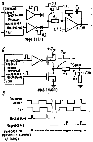
Type 2 phase detectors are sensitive only to the relative position of the edges of the input signal and the signal at the output of the VCO, as shown in Figure 3. Depending on whether the edge of the VCO output signal appears before or after the edge of the reference signal, the output of the phase comparator will generate lead or lag pulses, respectively.
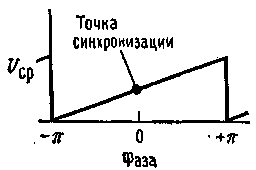
The duration of these pulses, as shown in the figure, is equal to the time interval between the edges of the corresponding signals. During the action of the lead or lag pulses, the output circuit respectively drains or gives current, and the average voltage obtained at the output depends on the phase difference, as shown in Fig.4. The operation of this circuit is completely independent of the duty cycle of the input signals (in contrast to the type 1 phase comparator circuit discussed above). Another advantage is that there is no output at all when the input signals are in sync. This means that there is no "ripple" at the output, which causes periodic phase modulation in type 1 phase detectors.
Here are the comparative characteristics of the two main types of phase detectors: Table 1
There is another difference between these two types of phase detectors. The output of a type 1 detector always requires subsequent filtering in the control loop (see below for more on this). Thus, in a type 1 detector PLL, the loop filter acts as a low-pass filter, smoothing full amplitude logic signals. In this case, residual pulsations are always present, the result of which are periodic phase oscillations. In circuits where the PLL is used for frequency multiplication or synthesis, this results in "lateral phase modulation" of the output signal. A type 2 detector, in contrast, generates output pulses only when there is a phase mismatch between the reference signal and the VCO signal. If there is no mismatch, the detector output behaves like an open circuit, and the loop filter capacitor acts as a storage device, storing the voltage at which the VCO maintains the desired frequency. If the frequency of the reference signal changes, the phase detector will generate a series of short pulses that will charge (or discharge) the capacitor to the new voltage needed to bring the VCO back into sync. Voltage controlled generators. An important component of the phase locked loop systems is the oscillator, the frequency of which can be controlled from the output of the phase detector. Some PLL ICs include a VCO, such as the 565 line element and a 4046 CMOS element. There are also separate VCO ICs, such as the 4024 (in addition to the 4044 TTL phase detector mentioned above), or various 74xx series TTL elements (for example, , 74S124 and 74LS324-327). Another interesting class of VCOs are oscillators with a sinusoidal output (8038, 2206, etc.). They generate a pure sine wave with distorted input signals. Table 2 provides a summary of the different VCOs. Table 2
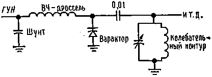
Note that the VCO frequency is not subject to the limitations of logic circuits. For example, you can use a radio frequency generator with a varactor (variable capacitance diode) (Fig. 5).
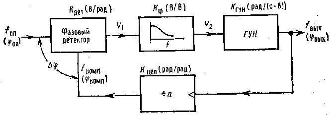
Without dwelling on this in detail, we note that even a microwave (GHz) generator based on a reflective klystron can be used, which is tuned by changing the voltage across the reflector. Naturally, a PLL device with oscillators of this type must contain an RF phase detector. PLL systems do not require the VCO to be too linear in frequency versus voltage. However, with significant nonlinearity, the transmission coefficient will change with frequency, and a greater margin of stability will have to be provided. PLL design Closing the control loop. At the output of the phase detector, an error signal is generated, associated with the presence of a phase difference between the input and reference signals. The VCO input voltage controls its frequency. It may seem that to create a closed control loop, it is enough to cover it with a feedback circuit with a certain gain, as is done in circuits with operational amplifiers. Here, however, there is one significant difference. In conventional circuits, the amount that is controlled by the feedback is the same as, or at least proportional to, the amount that is measured to generate the error signal. For example, in an amplifier, the output voltage is measured and the input voltage is adjusted accordingly. Integration takes place in the PLL system. We measure the phase, and we act on the frequency, and the phase is the integral of the frequency. This results in a 90° phase shift in the control loop. Since the integrator introduced into the loop feedback path introduces an additional 90° phase lag, self-excitation can occur at frequencies where the overall loop gain is unity. The simplest solution is to exclude from the circuit all other elements that give a phase delay at least at frequencies where the overall loop gain is close to unity. After all, op amps are 90° out of phase over almost their entire frequency range and still perform well. This is the first approach to solving the problem, the result of which is the so-called "first order contour". It is similar to the PLL block diagram above, but without the low-pass filter. Although such first-order systems are used in many cases, they do not have the necessary "flywheel" properties, that is, smoothing out noise or fluctuations in the input signal. In addition, since the output of the phase detector directly controls the VCO, a constant phase relationship between the VCO output signal and the reference signal cannot be maintained in the first order loop. The second-order loop to prevent instability contains an additional low-pass filter in the feedback loop. Due to this, a smoothing property occurs, the capture range narrows and the capture time increases. Moreover, as will be shown below, a second-order loop with a type 2 phase detector provides synchronization with zero phase difference between the reference signal and the output of the VCO. Second-order loops are used almost everywhere, because in most applications the PLL system must provide small fluctuations in the phase of the output signal, as well as have some memory or "flywheel" properties. Second-order circuits allow high gain at low frequencies, which gives increased stability (similar to feedback amplifiers). Now let's look at an example of using the PLL. Frequency multiplier. Development example. PLL systems are often used to generate signals whose frequency is a multiple of the input frequency. In frequency synthesizers, the output frequency is obtained by multiplying an integer n by the frequency of a stabilized low-frequency reference signal (for example, 1 Hz). The number n is set in digital form, and the tunable number generator can be controlled from a computer. In more prosaic cases, you can find the use of a PLL device to generate a clock frequency synchronized with some reference frequency already available in this device. Suppose, for example, that a two-stage ADC needs a clock signal at 61,440 kHz. At this frequency, 7,5 measurements per second are obtained; the first stage will last 4096 clock cycles (recall that in two-stage ADCs the duration of this stage is constant), and the maximum duration of the second stage will be 4096 cycles. A characteristic feature of the PLL circuit is that the clock signal with a frequency of 61,440 kHz can be synchronized to the mains frequency of 60 Hz (61,440=60x1024), which allows you to completely suppress mains interference at the converter input. Let us first consider the standard PLL circuit (Fig. 6), which contains an additional counter - a frequency divider by n, connected between the VCO output and the phase detector.
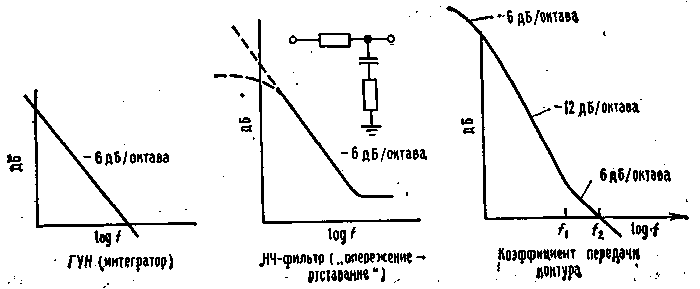
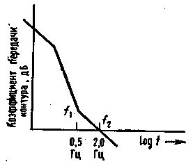
The diagram shows the transfer coefficients of each functional element of the circuit, which will help us in calculating the stability. We especially note that the phase detector converts the phase into voltage, and the VCO, in turn, converts the voltage into the derivative of the phase with respect to time, that is, into frequency. Thus, it can be considered that if we consider the phase as an input variable, then the VCO acts as an integrator. A fixed error input voltage causes a linearly increasing phase error at the output of the VCO. The low pass filter and frequency divider by n have gains less than one. Stability and phase shifts Figure 7 shows the Bode diagrams that allow us to evaluate the stability of the second-order PLL.
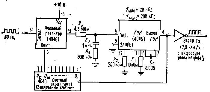
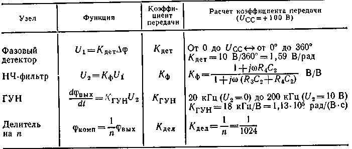
The VCO operates as an integrator with a time constant of 1/f and a 90° phase lag (i.e. the time constant is proportional to 1/jw and the capacitor is charged by the current source). In order to create a phase margin (the difference between 180 ° and a phase shift at a frequency at which the overall gain of the circuit is equal to 1), a resistor is connected in series with the capacitor in the low-pass filter, preventing stability breakdown at some frequencies (introducing "zero" of the transfer functions). Combining the VCO and filter characteristics gives the Bode diagram for the overall loop gain shown in the figure. As long as the slope is 6 dB/octave (in the unity gain region), the loop will be stable. This is achieved by using a lead-lag low-pass filter and with the right choice of its characteristics (as well as in the lead-lag phase compensation circuits of operational amplifiers). In the next section, we will show how this is done. Transfer coefficient calculation Figure 8 shows the PLL circuit for a frequency synthesizer of 61 Hz. The phase detector and VCO are part of a PLL based on a 440 type CMOS IC.
In this circuit, a version of the phase detector operating on the fronts is used, although the IC 4046 has both options. The output of the circuit is formed by a pair of pulsed CMOS transistors that provide pulsed signals of Ucc or 0 V levels. In fact, it is a three-state output considered earlier, since, except for the moments of the phase error pulses, it is in a high state. output resistance. The maximum and minimum VCO frequencies, set by the control voltage levels of 0 V and Ucc, are determined by the choice of resistors R1 and R2 and capacitor C1 according to the rating data. From the technical data for element 4046, one can determine a significant drawback of the circuit: high sensitivity to the stability of supply voltages. The choice of other elements of the contour is carried out according to standard procedures for the PLL. Once the VCO range is selected, all that remains is to design the low-pass filter, which is a very critical part of the system. Let's start by calculating the gain of the entire control loop. Table 3 shows the calculation formulas for individual components (according to Fig. 6). Table 3. Calculation of the PLL gain Calculations should be made carefully, not confusing the frequency f and the circular frequency w or hertz with kilohertz. Until now, we have not determined only the coefficient Kj. It can be determined by writing an expression for the overall gain of the loop, but first remember that the VCO is an integrator and write:
Hence the overall gain is
Now we choose the frequency at which the gain becomes equal to unity. The idea is that the single transmission frequency is chosen high enough so that the loop can properly track changes in the input frequency, but also low enough to smooth out noise and spikes in the input signal. For example, a PLL system designed to demodulate input FM signals or to decode a sequence of high-speed tones must be fast (for FM signals, the loop bandwidth must match the input signal, that is, equal to the maximum modulation frequency, and for tone decoding, the time constant loop must be less than the duration of the tone). On the other hand, since this system is designed to track certain values of a stable or slowly changing input frequency, it must have a low single transmission rate. This will reduce phase "noise" at the output and provide insensitivity to interference and glitches at the input. Even brief interruptions of the input signal will be barely noticeable, as the filter capacitor will store the voltage, which will cause the VCO to continue producing the desired output frequency. Taking into account what has been said, we choose the frequency of a single transmission f2 equal to 2 Hz, or 12,6 rad/s. This is well below the reference frequency, and it is unlikely that mains frequency deviations could exceed this value (recall that electrical energy is produced by large generators with huge mechanical inertia). The break point of the low-pass filter characteristic (its "zero") is chosen, as a rule, at a frequency less than f2 3-5 times, which provides sufficient phase margin. Recall that the phase shift of a simple RC circuit varies from 0 to 90° in the frequency range from 0,1 to 10 relative to the frequency of -3 dB ("poles"), at which the shift is 45°. So, let's choose the zero frequency equal to 0,5 Hz, or 3,1 rad/s (Fig. 9). The break point f1 determines the time constant R4C2 : R4C2=1/2pf1. Let's preliminarily accept: C2=1 uF and R4=330 kOhm. Now it remains only to choose the value of the resistance R3 from the condition that the transmission coefficient at the frequency f is equal to unity2. Having done this operation, we find that R3 \u4,3d XNUMX MΩ.
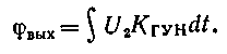
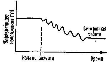
An exercise. Check that with the filter components selected, the gain at f2=2,0 Hz is indeed 1,0. Sometimes the obtained values of the filter parameters are inconvenient and you have to recalculate them or slightly shift the unity gain frequency. These values are acceptable for a CMOS PLL (typical VCO input resistance is 1012 Ohm), and for a PLL on bipolar transistors (type 4044, for example), you may need to match the resistance using an operational amplifier. To simplify the design of the filter in this example, a Type 2 edge-switched phase detector was used. This solution may not be the best in practice due to the high level of network interference. By careful selection of the analog input circuit (for example, a Schmitt trigger can be used), good circuit performance can be achieved. Otherwise, it is recommended to use XOR type 1 phase detector. Trial and error method There are people for whom the art of designing electronic circuits is to change the filter parameters until the circuit works. If the reader is one of them, then he should change his approach to this issue. Probably because of such developers, PLL systems have a bad reputation, and that is why we have given a detailed calculation. Nevertheless, let's try to help developers using the trial and error method: R3C2 determines the smoothing time of the contour, and the ratio R4 / R3 - damping, that is, the absence of overload during frequency hopping. We recommend starting with R4=0,2R3. Clock generation for video terminals A high-frequency generator synchronized with a network frequency of 60 Hz can be successfully used to generate clock signals in alphanumeric computer terminal equipment. The standard output speed of information on video displays is 30 frames per 1 s. Since network interference is almost always present, even if it is small, the image begins to experience slow "rolling". This happens if there is no exact synchronization between the mains frequency and the vertical channel of the display. A good way to solve this problem is to use the PLL system. In this case, a high frequency VCO (with a frequency of about 15 MHz, a multiple of 60 Hz) should be used, and the signals obtained by dividing this main high frequency clock sequence should be used to sequentially form the points of each character, line length and number of lines in the frame. PLL capture and tracking Obviously, the PLL will remain in synchronism as long as the input signal does not fall outside the allowed range of the feedback signals. An interesting question is the initial entry of the system into synchronism. The initial frequency mismatch produces a periodic difference frequency signal at the output of the phase detector. Ripple will decrease after filtering and a constant error signal will appear. Capture process. The answer to the question is not so simple. First-order control systems will always be in synchronism, since there is no attenuation of the error signal at low frequency. The second order loops can be both in sync and out of sync, depending on the type of phase detector and the bandwidth of the low-pass filter. In addition, the XOR type 1 phase detector has a limited acquisition bandwidth that depends on the filter time constant. This circumstance can be used if it is necessary to build a PLL system that must perform synchronization only in a certain frequency range. The locking process is as follows: when the phase error signal causes the VCO frequency to converge to the reference frequency, the error waveform changes more slowly and vice versa. Since this signal is asymmetric, slower changes occur in the part of the cycle in which fgun approaches fop. As a result, a non-zero average DC voltage puts the PLL into lock mode. The VCO input voltage changes during the capture process, as shown in Figure 10. Notice the last spike (overshoot) in the chart; the reason for it is very interesting. Even if the VCO frequency reaches the required value (as indicated by the voltage level at the VCO input), this does not mean that the system has necessarily entered lock, since it may turn out that there is no common mode. This may cause the curve to overshoot. It is obvious that the capture process in each case will occur differently.
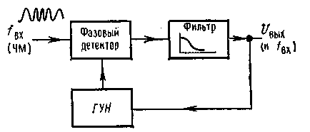
Strip of capture and tracking If a type 1 XOR phase detector is used, the acquisition bandwidth is limited by the time constant of the low-pass filter. This makes a certain sense, since if there is a large initial difference in frequency, the mismatch signal will be attenuated by the filter so much that capture can never occur. Obviously, increasing the time constant of the low-pass filter narrows the capture band, which is equivalent to decreasing the loop gain. It turns out that there are no such restrictions in a phase detector operating along fronts. The tracking bandwidth for both types of circuits depends on the VCO control voltage range. Some examples of the use of PLL systems We have already mentioned the use of PLLs in frequency synthesizers and frequency multipliers. As for the latter, the expediency of using the PLL, as can be seen from the considered example, is so obvious that there should be no doubts about the use of the PLL. Simple multipliers (i.e., high-frequency clocks for digital systems) do not even have problems with reference jitter, and first-order systems can be used quite well. Let's look at some applications of the PLL that are interesting from the point of view of a variety of areas of use. FM signal detection With frequency modulation, information is encoded by changing the frequency of the carrier signal in proportion to the change in the information signal. There are two methods for recovering modulated information: using phase detectors or PLL. The term "detection" here refers to a demodulation method. In the simplest case, the PLL is synchronized with the incoming signal. The voltage that is applied to the VCO and controls its frequency is proportional to the input frequency and therefore is the required demodulated signal (Figure 11). In such a system, the filter bandwidth must be chosen wide enough to allow the modulated signal to pass through. In other words, the PLL response time should be short compared to the range of the reconstructed signal. The PLL should not be fed a signal that is transmitted over a communication channel; here you can use the "intermediate frequency", which is obtained in the mixer of the receiver when converting the frequency. This FM detection method requires a highly linear VCO to avoid distortion at audio frequencies.
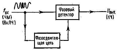
The second FM detection method uses only the phase detector and not the PLL. The principle is illustrated in Figure 12. The original input signal and the same phase-shifted signal are applied to the phase detector, at the output of which a certain voltage appears.
The phase shift circuit changes the phase shift linearly with frequency (usually done with resonant LC circuits). Thus, the demodulator output signal is linearly dependent on the output frequency. This technique is called "double balanced quadrature FM detection". It is used in many ICs to implement the intermediate frequency amplifier / detector path (for example, the CA3089 type). AM signal detection Let's consider methods that provide proportionality between the output signal and the instantaneous value of the amplitude-high-frequency signal. Usually, straightening is used for this (Fig. 13).
Figure 14 illustrates the original method using the PLL "("homodyne detection method"). The PLL system generates rectangular pulses of the same frequency as the frequency of the modulated carrier. After multiplying the input signal by the output signal of the PLL, a kind of full-wave rectification is obtained, after then it remains only to remove the rest of the carrier frequency with a low-pass filter to obtain a modulated envelope.If an XOR phase detector is used, then the output signal is 90 ° out of phase with respect to the reference signal.Therefore, between the PLL and the multiplier, you must include phase-shifting circuit with a phase shift of 90 °.
Clock synchronization and signal recovery. In digital signal transmission systems, information is transmitted in serial form over a communication channel. This information may be digital in nature or be the digital equivalent of analog information, as is the case with pulse code modulation (PCM). A similar situation arises when decoding digital information from a magnetic tape or disk. In both cases, interference or changes occur frequency of the pulses (e.g. due to tape pull) and it is required to obtain an undistorted clock signal of the same frequency as the frequency of the incoming information.PLL systems are recommended in this application, since a low-pass filter, for example, would only help to eliminate noise and pickup, but would not be able to track slow changes in tape speed. Literature:
Authors: Paul Horowitz, Harvard University, Winfield Hill. Publication: N. Bolshakov, rf.atnn.ru
Artificial leather for touch emulation
15.04.2024 Petgugu Global cat litter
15.04.2024 The attractiveness of caring men
14.04.2024
▪ Named the cause of concussion ▪ Wound healing without scar tissue ▪ Bacteria found that converts methane into electricity
▪ section of the site Your stories. Article selection ▪ article Time, forward! Popular expression ▪ propane soldering article. home workshop ▪ article Silk dyeing. Simple recipes and tips ▪ article Shrinking coin. Focus Secret
Comments on the article: Karen [up] class
Home page | Library | Articles | Website map | Site Reviews
www.diagram.com.ua |


 Leave your comment on this article: