|
|


 Arabic
 Bengali
 Chinese
 English
 French
 German
 Hebrew
 Hindi
Hindi Italian
 Japanese
 Korean
 Malay
Malay Polish
 Portuguese
 Spanish
 Turkish
 Ukrainian
 Vietnamese
|
ENCYCLOPEDIA OF RADIO ELECTRONICS AND ELECTRICAL ENGINEERING Memory chips from STMICROELECTRONICS. Reference data
Encyclopedia of radio electronics and electrical engineering / Application of microcircuits The article provides an overview of various types of memory developed and manufactured by STMicroelectronics, one of the world's leading manufacturers of electronic components, including memory chips, and which has a unique technology for the production of Flash-memory and programmable memory systems on a single chip. Currently, STMicroelectronics (ST) develops and commercially manufactures the following types of memory chips: EPROM - memory with ultraviolet erasure and one-time programming, including standard memory chips such as OTP и UV EPROM advanced memory chips OTP и UV EPROM family Tiger range, chips of a new family of memory Flexible ROM designed to replace MaskROM, as well as memory chips PROM и RPROM WSI (USA), which became part of ST; EEPROM и SERIAL NVM (serial non-volatile long-term memory) - memory chips are produced from serial reprogrammable non-volatile memory EEPROM with different bus interface, serial chips Flash -memory, standard special-purpose memory chips (ASM) and contactless (CONTACTLESS MEMORIES) memory chips; Flash memory type NOR - ST manufactures Flash-memory chips: industry standard with different power supply, with extended architecture for various applications, heterogeneous memory chips and Flash-memory chips of the family " Light Flash "; Flash memory type NAND - a new direction in the production of memory chips ST. SRAM - ST produces asynchronous low-power SRAM memory chips with different power supply and speed; NVRAM - There are various solutions for battery backed SRAM, which are classified as Supervisors, Zeropower, Timekeeper and Serial RTC; PSM - In accordance with the strategic direction of creating systems on a chip, ST develops and manufactures programmable memory system chips that provide a comprehensive memory system solution for microcontrollers and DSP designs; Smart Card - a wide range of chips for Smartcard and security systems is available. A large number of types and types of memory chips produced by ST does not allow their detailed coverage even within the framework of one review article. Therefore, here we will try to dwell only on the main features of some families of ST memory chips from those shown in Fig. one.
ST is one of the world's leading memory manufacturers. OTP и EPROM with UV erasing, which is convenient for designing, manufacturing and replacing mask ROMs because they are programmed at the end of production. The manufactured microcircuits have a capacity from 64 kbps to 64 Mbps with a power supply of 5 and 3 V, sufficient speed, various packages, including those for surface mounting. Device memory organization can be of type x 8, x 16 and x 8 / x 16. Deciphering the designations of ST memory chips of the form OTP и UV EPROM shown in Fig. 2. The product portfolio includes standard 5V and 3,3V ICs, advanced ICs of the family Tiger Range with 3 V power supply (2,7-3,6 V) and microcircuits of a new family FlexibleROM™. These memory types are available in FDIP ceramic windowed and PDIP plastic double-row packages, as well as surface mount PLCC and TSOP packages. For low voltage series Tiger Range ST used the latest technology OTP and UV EPROM. Structural improvements related to the thickness of the base layers have made it possible to significantly improve the electrical performance. A 25% reduction in the thickness of the gate oxide layer made it possible to lower the cell threshold voltage and increase the sampling rate when powered by 2,7 V. STMicroelectronics strives to provide consumers with new products with improved electrical characteristics, and therefore recommends that customers replace the "V" series with a power supply of 3 - 3,6 V with the "W" series - Tiger range, which has the best characteristics when supplied with a power supply of 2,7 - 3,6 V. Timing parameters for the series Tiger Range guaranteed by double testing the chips at 2,7V and 3V. The access time at 2,7V is marked on the chip and the faster access time is specified in the description. Access times for supply voltages above 2,7 V are valid. family UV and OTP EPROM Tiger Range characterized by ultra-low consumption, high operating speed and at the same time fast access with short programming times. Chip programming time is the same for both word and byte programming modes. For the latest chips with a density of 4 MB and 8 MB, the programming speed has been increased to 50 µs per word or byte. Microcircuits of the low-voltage series Tiger Range fully pin compatible with standard 5V series UV и OTP EPROM . This ensures that they are fully compatible for applications where microprocessor power is changed from 5V to 3V.
ST's EPROM technology is constantly being improved. New perspectives are opening up with the introduction of a new memory chip architecture based on the use of multi-bit memory cell technology to achieve high recording densities, starting from a capacity of 64 M bits. In addition, each new development contains several photolithographic innovations that improve the electrical performance of microcircuits. With the entry into STMicroelectronics of WAFERSCALE INC (USA), the possibility of supplying memory chips of the type PROM (programmable ROM) / RPROM (re - programmable ROM). These chips are available in three operating temperature ranges: commercial (0 to + 70° C), industrial (-40 to + 85° C) and military (-55 to + 125° C). In addition, some components are manufactured to the military grade (SMD) standard, including the EPROM. The latest development of STMicroelectronics in the field of electrically programmable ROMs is a family of FlexibleROM™, which can be used as a simple replacement for any ROM. This single-use programmable family, manufactured using ST's 0.15 micron technology, is available to the consumer with an initial memory capacity of 16 M bits. The new family of memory chips "FlexibleROM" is a type of non-volatile memory and is designed to store program code. "FlexibleROM" - ideal for use instead of mask ROM (MaskROM) and transition from Flash memory to ROM after debugging the program, if there are no plans to change the program code in the future. Thanks to Flash-based technology, programming time is also greatly reduced. The FlexibleROMs are provided with a generic high data rate verbose program capability, which allows programming a 64M bit device in as little as nine seconds. Another advantage over other One-Time-Program ROMs is high programming throughput, as 100% of the functionality of the memory array is verified during testing. The FlexibleROM memory family uses a supply voltage of 2,7 V to 3,6 V for read operations and 11,4 V to 12,6 V for programming. The devices have a 16-bit organization, by default the memory mode is set to “Read” at power-up, so they can be read as ROM or EPROM. Serial Non-Volatile Memory - the most flexible type of non-volatile non-volatile memory, which provides the ability to write down to the byte level, without the need to erase data before writing a new value. This makes them ideal for storing parameters. ST's Serial Flash memory families have "sector erase/page flash" and "page erase/page flash" capabilities. This is made possible by the finer grain size of the memory compared to standard Flash memory, which does not have the same grain size as the byte level of a serial EEPROM. ST has rich experience in using serial memory chips in home appliances. It occupies a leading position in the production of memory chips for automotive electronics, as well as for the computer components and peripherals market. These areas are the main consumers of long-term memory chips. This year for EEPROM the company uses 0.35 micron manufacturing technology, which allowed to bring the memory capacity up to 1 Mbps in accordance with the needs of the market. At the same time, the manufacturing technology of serial Flash memory has reached the level of 0.18 microns, and it became possible to manufacture this type of memory completely in accordance with market demands. The ST serial NVRAM portfolio includes a range of circuits from 256 bits to 16 Mbits. All ST memory chips are provided with descriptions, application examples and model files, making them easy to use. ST serial non-volatile memory chips are available in five voltage ranges: from 4,5 V to 5,5 V, from 2,5 V to 5,5 V, from 2,7 V to 3,6 V, from 1,8 V to 5,5 V and 1,8 V to 3,6 V. Design durability EEPROM - more than a million rewrite cycles with data safety for more than 40 years. Chips are produced in various packages, including traditional PSDIP, TSSOP, SO, as well as modern LGA and SBGA (thin film) types. In addition, it is possible to supply chips in packages on a drum and in unsawn form. ST Microelectronics manufactures a wide range of high quality serial memory eeprom, with densities from 1 KB to 1 MB, with three industry serial bus standards (400 kHz, I ? C, 2-wire bus with a density of up to 1 M bits, fast 1 M Hz bus type MICROWIRE (r) with a density from 1 kbps to 16 kbps and an ultra-fast 10 MHz SPI-type bus with a density up to 256 kbps), with a power supply of 5 V, 2,5 V and 1,8 V. The serial EEPROM notation for typical packages is shown in Figure 3. For not sawn plates and microcircuits in drums, the designations may differ slightly.
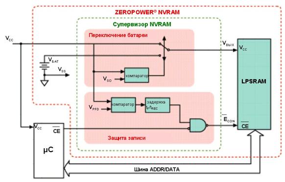
Microcircuits consistent EEPROM with bus I2C recommended for use in applications that do not require high bus speeds for accumulating and storing data, but want to have the ability to byte and page read/write. The bus operates at a clock speed of 400 kHz with supply voltages up to 1,8 V. Serial EEPROM is available from ST in a variety of packages: plastic DIP dual-in-line, SO, MSOP, TSSOP surface mount and SBGA with ball pin array. Memory chips EEPROM with SPI bus preferred for high speed bus applications. With the advent of chips with speeds from 5 MHz to 10 MHz and capacities from 512 kbps to 1 Mbps, this bus is rapidly gaining popularity in the memory chip market. EEPROMs with SPI bus have input HOLD ("Capture"), which allows you to maintain synchronization during pauses in the process of transmitting data sequences on the bus. In addition, there is a special control input W to protect the memory matrix from writing. Memory chips EEPROM with bus MICROWIRE® available in capacities from 256 bits to 16 kbits. Currently, the MICROWIRE bus is widely used in many modern devices that require a sufficiently high data transfer rate without the use of external address/data buses. The ST family of high-speed, low-voltage serial Flash memory chips has a four-wire SPI-compatible interface, allowing Flash memory to be used instead of serial EEPROM. Manufactured using highly durable CMOS Flash technology, these chips provide at least 10000 reprogramming cycles per sector with over 20 years of data retention. There are currently two complementary subfamilies of sequential flash memory with sector or page erasure capabilities: Serial Erase Flash with Page Programming: M 25 Pxx series (fully in production) Serial Flash Memory with Page Erasing and Programming: M 45 PExx series (this is a new series, samples available, full production in progress). When looking at different types of high-density serial non-volatile memory chips, the 25 MHz M25Pxx is significantly faster than many other types of serial flash memory chips. The ST Serial Flash family can load 1 MB of RAM in 43 ms with a minimum number of instructions, making them easy to use. Technical and software protections protect stored information from being overwritten. To reduce power consumption, these ICs operate from a single 2,7 V to 3,6 V power supply and have a low power mode that consumes less than 1 µA of current. In addition, the four-wire interface greatly reduces the number of device pins used to control bus communication, resulting in high integration and lower cost than other similar circuits. The M25Pxx series memory chips are available in wide and narrow S08, LGA and MLP packages. For evaluation and programming The M 25 PXX has a handy programmer/reader. This programmer connects directly to a PC and allows the user to directly access and control the M 25 xxx serial flash memory in any configuration. M45PExx is a series of high performance non-volatile memory chips with a higher grain size than before. Any page of 256 Bytes can be individually erased and programmed, and the Write command provides for the possibility of modifying data at the byte level. In addition, the architecture of the M45PExx is optimized to minimize the required application software. It takes 256 ms to write, 12 ms to program, or 2 ms to erase to modify one page of 10 bytes. This makes the M45PExx high-performance serial non-volatile memory chips very suitable for use in applications requiring the storage of large amounts of frequently changing data. Specialized memory chips have individual characteristics for specific applications or are designed in accordance with the requirements. They are based on standard memory arrays with specific I/O circuitry and specialized internal logic. These products are based on serial EEPROM and include logic for applications such as "Plug and Play" computer monitor with VESA standard, computer DRAM modules, etc. Among these microcircuits, one can note M 24164-16 K b cascaded EEPROM with special addressing, the possibility of using 8 devices in cascade on one bus and special addressing used in case of conflicts on the I 2 C bus. Another specialized chip that can be widely used in our market is M 34 C 00 - electronic board descriptor, designed to store small electronic notes about the board . The M34C00 can store the registration number, factory settings (default), user settings, data on events during the life of the board, information about failures and service maintenance of any board, etc. This chip has 3 banks of 128 bits (one is non-erasable ( OTP type), one standard EEPROM bank and one standard EEPROM bank with permanent write protection), two-wire I? C bus serial interface, power supply from 2,5 V to 5,5 V, SO 8 or TSSOP 8 housing, operating temperature range - 40 ... + 85°C. Contactless memory chips are a specific product. According to their classification, on the one hand, they can be attributed to specialized EEPROMs, and on the other hand, they can be distinguished as an independent type of memory, which has recently been widely used in various fields. ST has contributed to the development of a new ISO standard for contactless communication memory - ISO 14443 type B (implemented in microcontroller devices on Smartcards in transport and many other applications), as well as ISO 15693 and ISO 18000. ST now offers a new series of contactless memory chips and contactless communication chips with RF interface for applications such as tags, radio frequency identification (RFID) and contactless access systems using specialized memory chips. Let us note the features of some microcircuits of this type that are popular on the Russian market. Chip SRIX 4 K has 4096 user bits EEPROM with OTP, binary counter and write protection. Complies with ISO 14443-2/3 type B. It has an anti-cloning function patented by France Telecom. Operates at a carrier frequency of 13,56 MHz with a subcarrier frequency of 847 kHz, a frequency with a data rate of 106 kbps. Amplitude modulation (ASK) of data is used when transmitting from the reader to the card and binary phase modulation (BPSK) for transmission from the card to the reader. Chip LRI 512 has 512 bits with locking at the data block level. It fully complies with ISO 15693 (up to 1 meter) and E requirements. A. S. Operates at a carrier frequency of 13,56 MHz with 1/4 and 1/256 pulse coding at high and low data rates on one or two sub-carrier frequencies. Data amplitude modulation is performed during transmission from the reader to the card and Manchester coding is performed during transmission from the card to the reader. In a microchip CRX 14 There is a radio communication mechanism built into the chip with protocol and modulation according to ISO 14443 type B (radio interface). Features France Telecom's patented anti-cloning function. Provides serial access to the base at a frequency of 400 kHz over a two-wire serial bus I? C with the ability to connect on one bus to eight CRX 14. It has a 32-byte buffer for input and output packets and a built-in cyclic redundancy code calculator (CRC calculator). Available in S 016 Narrow (compressed) case. ST is one of the few companies that develops and produces non-volatile RAM chips (NVRAM). ST's solution to ensure the safety of RAM data during failures and loss of external power is to use a backup power supply (miniature lithium battery) located directly on top of the chip or on the system board. Based on the problems solved using RAM, ST produces four types of NVRAM chips: supervisors, ZEROPOWER® NVRAM, Serial RTC and TIMEKEEPER® NVRAM. There are two classes of supervisors: microprocessor supervisors (Microprocessor supervisor) and non-volatile ROM supervisors (NVRAM supervisor), and a combination of both classes is also possible. The main functions of the microprocessor supervisor (µ P) are voltage monitoring and watchdog function. Most microprocessor supervisors include these features. In combined microcircuits, integration of other functions is possible. The main functions of the NVRAM supervisor are voltage monitoring with battery switching and write protection. The voltage monitor protects the microprocessor (and system) by monitoring the power supply voltage and generating a signal RESET (RESET) for the transition of the microprocessor to the initial state at an unacceptably low value of the supply voltage. This option is called low Voltage Detect (LVD) - "Low voltage detection". At power-up, the voltage monitor also outputs a RESET signal until the supply voltage has stabilized. This option is called power- on Reset (por) - "Reset at power on". The built-in emergency battery switching circuit monitors the voltage of the external power supply. When it falls below a certain switching threshold, it switches to battery power, which provides continuous voltage to the low-power static RAM (LPSRAM) to store data in it. An integrated write protection circuit monitors the voltage of the external power supply and, when it falls below a certain threshold level, closes access to LPSRAM. Sometimes, to obtain non-volatile RAM, developers solve the problem of creating them instead of using existing modules. Standard low-power random access memory (SRAM) can be converted to NVRAM by adding a battery, write protection circuitry, and battery switching circuitry. ST has several devices that integrate all these functions. In addition, the battery and crystal are integrated into a SNAPHAT ® package, which simplifies the task of developing an NVRAM solution. Since uninterrupted power supply to the real-time clock requires a battery switch and a write protection circuit, it is natural to want to have a real-time clock in the NVRAM supervisor. ST has three microcircuits that have this combination - these are microcircuits M41ST85, M48T201 и M48T212 . All three of these devices also include microprocessor supervisor functions: POR, LVD, and watchdog. NVRAM supervisors with a real time clock are called "TIMEKEEPER® Supervisor. One of the latest ST developments is a chip M41ST87 in the SOX28 case designed for use in cash registers. This supervisor is specifically designed for applications requiring a high degree of data protection and security. Microcircuits M41ST87 combined with tamper detection circuits that erase memory contents within the supervisor to ensure the security of remote devices such as point-of-sale and credit card terminals. They integrate an NVRAM supervisor, a serial real-time clock, and a microprocessor supervisor into one new ST 28-pin SOIC (SOX28) package. In addition to the crystal, the SOX28 package also contains a 32 kHz quartz, which reduced the profile and size of the contact area of the microcircuit. Available in 3V and 5V power supply versions, the M41ST87 integrates many different functions and utilizes its own backup power supply from an external battery or normally found in systems, saving on cost as well. The intrusion detection circuitry has two independent inputs, each of which can be configured for several different connection schemes. Upon detection of the tampering phenomenon, user options include clearing the internal 128 bytes of RAM, sending an interrupt to the system microprocessor, and a dedicated signal pin to clear the external RAM. These features prevent an intruder from accessing sensitive data (eg, a user's password) contained in any RAM, as well as interrupting the system processor to be informed of a security breach. These functions are also provided when the M41ST87 chips are operated in battery-backed mode. Other security options include clock failure detection and automatic timestamping when tampering is detected. In addition, the M41ST87 provides the user with a unique 64-bit serial number. The M41ST87 chip package with embedded quartz also contributes to safety. In addition to saving space and the cost associated with system maintenance, quartz is closed from outside access. In addition, it is better protected from the effects of the natural environment. Taking into account all factors, it can be argued that such a solution by ST allows you to reduce the cost of the system as a whole. Chip NVRAM Supervisor M41ST87 can be used to manage low-power RAM. The following built-in circuits are used here: an automatic battery switch circuit, an access permission circuit (Chip - Enable Gate) to protect the RAM from writing, and a battery monitor. This allows the user to create an NVRAM using the M41ST87 backup battery to duplicate LPSRAM power. The M41ST87 is based on a programmable, battery-powered real-time clock with counter registers that tracks time and date with resolutions ranging from hundredths of a second to hundreds of years. They are accessed via the I 2 C interface with a frequency of 400 kHz. Formed using low power CMOS technology, the M41ST87 real time clock circuit RAM is organized as 256x8 bits, with 21 byte registers and has 128 bytes of native NVRAM plus 8 bytes dedicated to a unique serial number. The M41ST87 IC Supervisor includes two independent pre-warning circuits for power failure (PFI/PFO) with a 1,25V comparator reference, a reset circuit that can be triggered from multiple sources on two inputs, and a low voltage detection circuit that outputs a signal. reset. A watchdog timer with a programmable timeout from 62,5 ms to 128 s can also be used as a reset source. In addition, tamper detection circuits can also be configured as reset sources. One or both PFI/PFO circuits can be used not only to provide early warning of power failure, but also to control reclose circuits. Thus, up to three different supply voltages (including Vcc) can be controlled when using the M41ST87. The low-profile SOX28 package takes up little board space (2,4x10,42mm including pins). Chips M41ST87 operate in the industrial temperature range from -40 o C to +85 o C. For surface mount and high density RAM solutions, ST suggests using a separate supervisor and multiple LPSRAMs. Such a multi-chip solution often requires less board space than other solutions and is much lower in cost than hybrid DIPs. Users can connect different amounts of LPSRAM to the appropriate ST NVRAM Supervisor, allowing a wide variety of densities and capabilities to be configured. Typical combinations include: - 16Mbps, 3V or 5V SMT solution using M40Z300 supervisor without top battery with four M68Z512 low power RAMs; - 1Mbit or 4Mbit, 3V SMT solution using M40SZ100W SNAPHAT® supervisor and low power SRAM type M68Z128W or M68Z512W. Series ICs ZEROPOWER® got their name for their ability to save data in the absence of external mains power. They consist of two main components: low-power RAM (LPSRAM) and supervisor NVRAM (Figure 4). Typical LPSRAM typically consumes less than one µA when running on battery alone and can store data for several years when powered by a miniature lithium battery. The NVRAM supervisor consists of two main circuits: a battery switch circuit and a write protection circuit. The battery switching circuit switches the LPSRAM power supply from the system regulated power supply (Vcc) to battery power (Vbat). This circuit monitors Vcc and when it starts to drop, the LPSRAM power is switched to the backup battery.
When Vcc drops below a certain threshold value, the microprocessor may behave erratically, and this may lead to erroneous writes and even clear the contents of the RAM. The write protection circuit prevents the microprocessor from accessing the LPSRAM to prevent this situation. All microcircuits ZEROPOWER® NVRAM ST companies have the same capabilities and no other external circuitry is required. Currently, microcircuits are produced with NVRAM and LPSRAM supervisors integrated on the same chip with a density of up to 256 kbit and below. For higher densities, two separate microcircuits are still used.
ST's NVRAM chips are available in a variety of packages. The main surface mount package (SMT) is the package SNAPHAT® (Fig. 5a). The chip in the SOH 28 package has a standard SRAM pinout, and the battery is mounted on top with clasps, which makes it easy to replace. Housing type CAPHAT (Fig. 5b) has a non-removable battery. It is recommended for through hole applications. For through-hole solutions and high RAM density, a hybrid DIP package is available, in which the LPSRAM and supervisor are separate chips mounted on a common printed circuit board along with the battery (Figure 15c). RAM densities up to 16 M bits are currently available. With developers in mind, one of the latest ZEROPOWER ® NVRAMs is the M 48 Z 32 V chip in a low profile package. Chip M48Z32V features 32Kx8 LPSRAM memory density at 3,3V. Low profile 44-pin SOIC package rises just 0.12" (3,05mm) off the circuit board, giving users greater flexibility in board layout and eliminating size concerns for designers in height. Chip M48Z32V has a built - in battery backup switch and write - protection circuits in case of power failure combined with 256 kbit low - power SRAM . The access time for these chips is 35 ns for the M48Z32V-35MT1 and 70 ns for the M48Z32V-70MT1. Consuming only 200nA (typ. at 40°C), the M48Z32V can store data for ten years of battery life with a capacity of 18mAh. This chip is compatible with systems that already contain lithium batteries on the board. Combining a low-profile chassis with value M48Z32V allows it to be used as a successful NVRAM solution in many applications. By using its contacts to connect to any battery supply, the M48Z32V chip can be used as an ordinary asynchronous static RAM for any microprocessor or microcontroller. The M48Z32V is manufactured in a SO44 package, which is similar to the SOH44 SNAPHAT® type ST package, but without the top battery. It is powered by a 3,3V (±10%) supply and operates in the commercial temperature range (0 to 70°C).
Microcircuits TIMEKEEPER® NVRAM are based on the use of NVRAM ST core technology. Since ZEROPOWER ® NVRAM chips are battery powered, the addition of a real-time clock greatly expands the capabilities and applications of NVRAM chips. Your name TIMEKEEPER® such microcircuits were obtained precisely because of the presence of a real-time clock with a calendar, which gives the system the exact time, day and date even in the absence of external system power (Fig. 6). TIMEKEEPER ® NVRAM chips are based on ZEROPOWER ® NVRAM, to which is added real-time clock/calendar circuitry, including a 32 kHz crystal oscillator. The emergency power switching circuit used to store data in LPSRAM is also used for RTC. Similarly, in the interests of RTC write protection, the NVRAM write protection scheme is applied. The RTC generator is power optimized and its consumption does not exceed 40 nA. The operating principle of a real-time clock is to use a 32 kHz oscillator and then divide the frequency by several counters. The first counter divides the generator frequency by 32,768 and its output produces a signal with a frequency of one hertz. The next counter counts the number of seconds and sends a signal to the minute counter once a minute. The next successive counters continue to divide the frequency downwards until they produce one pulse per century. Additional logic is used to control the number of days in each month and account for leap years. The data at the outputs of the counters correspond to the current time and date. These parameters are transferred to the NVRAM distributed memory area and appear as ordinary addresses of RAM cells. Users read/write time and date by reading/writing these addresses in NVRAM space. Buffers provide "seamless" reading/writing of RTC data. When reading the RTC, a frame of captured data about the current real-time state is stored in buffers, from where the data is read by the microprocessor. The presence of a data frame guarantees the invariance of time during the next cycle of reading by the microprocessor. Similarly, during a write cycle, the buffers hold the data coming from the microprocessor and wait for the end of the day-date-time information write cycle to simultaneously transfer the incoming data to the hour counters. The RTC registers are mapped to LPSRAM. For this, from 8 to 16 bytes of LPSRAM are used. The day, date, and time are read and written as ordinary RAM addresses. Incorporating ZEROPOWER ® NVRAM, TIMEKEEPER ® NVRAM chips retain all their main features, including the absence of additional external circuits. With memory densities up to 256 kbps, the real-time clock and NVRAM supervisor are integrated on the same chip as LPSRAM. For higher memory densities, a separate LPSRAM chip is used. Depending on the execution technology, the components that make up the chip can be placed in one "hybrid" package, or on the same substrate in a separate IC package (the emerging technology of TIMEKEEPER ® packaging). Like TIMEKEEPER® NVRAM chips, serial real-time clocks (Serial RTC) keep track of the current real time even in the absence of external system power. Instead of the standard SRAM asynchronous parallel interface, serial RTCs use a serial bus. ST devices are available in two versions of the industry standard serial interface: I ? C and SPI. These chips are made based on TIMEKEEPER ® NVRAM by reducing the number of NVRAM to a few bytes and changing the interface to one of the standards listed above. Most devices Serial RTC contain a battery switch, write protection circuits, and many other modern microprocessor supervisory features such as power reset and watchdog timer (Figure 7). For applications that do not require redundancy or need only short-term redundancy using a capacitor, ST provides simpler and cheaper Serial RTC devices, such as M 41 T 0 и M 41 T 80 .
ST full-featured serial real-time clock ICs have many microprocessor supervisor functions. For example, M 41 T81 - this is Serial RTC with I interface2With 400 kHz, Alarm, programmable Watchdog, programmable square wave generator, in SO 8 or SOX28 SOIC type housing (with quartz built into the housing). Chip M 41 T 94 is the first Serial RTC ST device with SPI interface. It has integrated P O R / LVD circuits, programmable Watchdog, Alarm, the ability to connect a reset button. The chip is available in SO 16 and SOH 28 SNAPHAT ® packages. Serial RTC chip M 41 ST 84 with I interface2C 400 kHz is distinguished by the advanced capabilities of the microprocessor supervisor. In addition to P O R / LVD, Programmable Watchdog and Alarm functions, it provides Power Failure Early Warning (PFI / PFO) and Input Reset. Manufactured in SO 16 housing. Modern ST NVRAM chips have achieved such a level of integration that some of them (M41ST85, M41ST87 и M41ST95) can be classified as both Serial RTC and TIMEKEEPER® supervisors. The achieved level of integration now makes it possible to place quartz directly in a monolithic microcircuit package next to the crystal, and not to take it to the upper battery. An example of such a solution that improves reliability and security is a microcircuit М41ST85МХ6 . Along with highly integrated SERIAL RTC chips, ST produces devices containing the minimum necessary for continuous output to the real-time system. Microchips are such devices. M 41 T 0 и M 41 T80. They contain a full set of time counters and take into account the features of leap years. Additional features of these devices include a programmable alarm signal with interrupt processing, a programmable square wave output, and a separate 32 kHz signal output used as a reference input signal for clock generators of other chips. With these capabilities, these chips cover the application needs of a large portion of the consumer market. The M41T0 and M41T80 ICs have an industry standard I serial interface.2C 400 kHz and operate in the industrial temperature range from -40 o C to +85 o C. Manufactured in surface-mount packages, both devices operate from a power source with voltages from 2 V to 5,5 V with low current consumption. For example, the M41T0 only consumes 900 nA in standby mode and 35 µA in active mode (using a typical 3,0 V supply). The M41T80 consumes 1,5 µA in standby mode (with a typical supply voltage of 3,0 V) and only 30 µA in active mode (with a maximum supply voltage of 3,0 V). In addition to the main clockkeeping task, the M41T0 chip has an oscillator stop bit option to detect the frequency drift of the clock generator due to a decrease in the supply voltage. As for the M41T80, its timing properties are complemented by a programmable Alarm interrupt with snooze modes, a dedicated 32 kHz frequency output, and a programmable square wave output from 1 Hz to 32 kHz. The dedicated 32 kHz pin can be used to drive microprocessors and microcontrollers with a phase-locked clock circuit that requires 32 kHz as a reference. In addition, the same pin can be used for clock synchronization of microcircuits when they operate in low-power modes. The 32 kHz output is designed for continuous operation, but may be disabled by user software. The Alarm function of the M41T80 chip has a mode with Alarm repeating from once a year to once per second. The square wave programming function allows you to program its frequency from 1 Hz to 32 kHz with a multiplier of 2.
The M41T80 chip is easily connected on the I bus2C 400 kHz with almost any microprocessor and microcontroller (Fig. 8), and with the addition of an external diode and capacitor, it can always support the microcontroller during a momentary power failure. Since bus I2C works with open drain, then there is no problem in voltage matching between the microprocessor and the M41T80, and it is enough to use one diode for voltage decoupling. When using a 1 F capacitor and a Vcc supply voltage of 3,3 V, the expected backup time is approximately 10 days. The M41T80 ICs are available in a small size SO8 package. Also available in TSSOP8 package. The simplest device from the SERIAL RTC ST series of chips is a chip M 41 T0, developed on the basis of M41T00, M41T0. This device does not have a battery switch and software clock calibration, but has a generator failure detection function and an I interface2C from 400 kHz. Chip M41T0 when using an external 1 F capacitor at 3,3 V, it can provide backup power for up to two weeks. The upper battery for ST NVRAM chips is supplied separately and this must be taken into account when ordering these circuits. NVRAM memory chips are also produced by other companies, but many of them do not have the features that are inherent in ST components. NVRAM STMicroelectronics chips are distinguished primarily by higher integration, the presence of a built-in battery switch and the ability to software calibrate the clock, for which software is used (available on the ST website). Publication: cxem.net
Machine for thinning flowers in gardens
02.05.2024 Advanced Infrared Microscope
02.05.2024 Air trap for insects
01.05.2024
▪ Apple moves computers to its own processors
▪ section of the site Experiments in chemistry. Article selection ▪ article Road traffic injuries. warning rules. Basics of safe life ▪ article How does a chameleon change its colors? Detailed answer ▪ Anchar article. Legends, cultivation, methods of application
Home page | Library | Articles | Website map | Site Reviews
www.diagram.com.ua |


 Leave your comment on this article: