|
|


 Arabic
 Bengali
 Chinese
 English
 French
 German
 Hebrew
 Hindi
Hindi Italian
 Japanese
 Korean
 Malay
Malay Polish
 Portuguese
 Spanish
 Turkish
 Ukrainian
 Vietnamese
|
ENCYCLOPEDIA OF RADIO ELECTRONICS AND ELECTRICAL ENGINEERING End stage UMZCH. Encyclopedia of radio electronics and electrical engineering
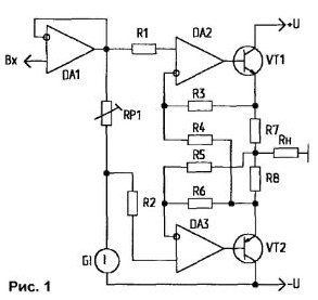
Encyclopedia of radio electronics and electrical engineering / Transistor power amplifiers In my previous designs, I used the output stage of the current amplifier according to the circuit from [1] with the class "A *" mode. Over time, there was a desire to make a 2-band power amplifier with an active crossover filter. And given that switching distortions are especially pronounced at high frequencies, it is advisable to use the class "A" mode, which excludes this type of distortion. But making another amplifier with "A" mode is very cumbersome and expensive. Basically, it's two amps in one. In the digest "Radiohobby" [2], a circuit of the UMZCH output stage with class "A" linearity, but thermal stability and class "AB" efficiency, developed by Mike Renardson, was published. The author managed to combine two ideas previously published in the Radio magazine. Firstly, implemented in the UMZCH circuit by Yu. Mitrofanov [3], which ensures the absence of switching distortions at a quiescent current corresponding to the "AB" mode. Secondly, in L.Kompanenko's circuit [4], using an operational amplifier to stabilize the voltage drop across the resistor in the emitter circuit of the output transistor, which ensures the stability of the quiescent current. On this basis, the UMZCH output stage circuit without a common negative feedback was developed. Figure 1 shows a functional diagram of the feedback that ensures the operation of the transistor VT1 without cutoff (in class A mode). At the same time, the transistor VT2 operates in the normal mode (with collector current cutoff and during the blocking half-cycle of the input voltage). Op-amps DA1 and VT1 form a signal inverter at the VT2 emitter, so any non-linearity of the lower arm is compensated by a highly linear upper arm. In addition, op amps DA3 and VT2 provide stabilization of the quiescent current, set by the voltage drop across the resistor RP1.
On fig. 2 shows a complete diagram of the UMZCH output stage.
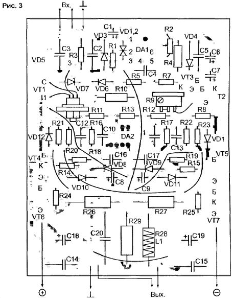
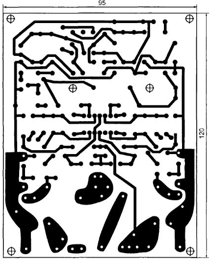
The voltage-amplified input signal is fed through a decoupling capacitor C3 and an "anti-ringing" resistor R6 to the gate of the source follower on VT1, the operating point of which is maintained in class "A" mode by a stable current generator on transistors VT2 and VT3. A resistor R10 is included in the source circuit, which sets the bias voltage at the bases of the output transistors. From this resistor, the signal is fed to the non-inverting inputs of the op-amp DA2.1 and DA2.2. These op amps provide coverage of the OOS base-emitter transitions of the output composite transistors VT4-VT6 and VT5-VT7. Given that the speed of the output transistors is lower than the op-amp, corrective circuits R18-C16 and R19-C17 are introduced. limiting the frequency band of the signals supplied to the bases of the transistors. To ensure the stability of the output stage, the gain of the op-amp is reduced and the frequency band is limited by the introduction of chains R16-C12 and R17-C13. The economical mode of operation of the output transistor VT6 is obtained by connecting the inverting input DA2.1 to the emitters of transistors VT6, VT7 of both arms of the 2-stroke output stage. This ensures that the quiescent current flows through VT6 even during the blocking half-cycle of the input voltage. The inverting input of another op-amp DA2.2 is connected to a resistor R27 in the VT7 emitter circuit and provides stabilization of the quiescent current of the output transistors. The quiescent current of the output transistors V16 and V17 is set by the voltage drop across the resistor R10, and it is adjusted by changing the current through R10 by the resistor R9. Zero balancing in the output of the stage is provided by an integrator on DA1 with a trimming resistor R2. The DAT power source is a parametric stabilizer on zener diodes VD3 and VD4. Diodes VD5. VD6 and Zener diode VD7 protect the gate of the field-effect transistor VT1 from breakdown when using high-voltage voltage amplifiers on lamps or transistors [5]. DA2 is powered from a parametric stabilizer on zener diodes VD8, VD9, and the tracking synchronous power is supplied to the common point of the zener diodes from the output of the source follower to VT1. The amplifier is placed on the board, the drawing of which is shown in fig. 3. In principle, only domestic components are used in this scheme, although there are no restrictions on replacing them with imported analogues, with the exception of DA2 (K157UD2), which has no direct analogues.
When working out the circuit as VT6, VT7, transistors KT818G, KT819G were used. Their subsequent replacement with imported 2SA1302, 2SC3281 had practically no effect on the sound quality. Output transistors VT4, VT6 and VT5. VT7 are installed in pairs on heat sinks with an area of about 300 cm2 each. Transistors VT1 and VT3 are equipped with small (about 5 cm2) plate heat sinks made of 2 mm thick aluminum sheet. The resistors that determine the OOS parameters (R20 ... R23. R26. R27) must be with a tolerance of 1% or selected with a resistance spread of about 1%. Setting. First, set zero at the output of the UMZCH with a tuning resistor R2, and then the required quiescent current of the output transistors with R9. More precisely, it can be set by applying a 2-tone sinusoidal signal with a difference frequency of 1 kHz (for example, 10 and 11 kHz or 19 and 20 kHz) to the input, and connecting a low-power (1-2 W) full-range speaker to the output. At zero quiescent current (maximum resistance R9), a difference tone with a frequency of 1 kHz is clearly audible. As the quiescent current increases, it decreases to a barely audible level. If a further increase in current does not lead to a decrease in the sound level, this is the end of the tuning. The quiescent current of the output transistors VT6. VT7 is practically independent of the temperature of their cases and only slightly changes with the heating of transistors VT1 and VT3. And since they have opposite temperature dependences of the current transfer coefficient and operate in class "A" mode with constant heat release, a slight change in the voltage across the resistor R10 occurs only during warm-up and does not change in the future. Comparisons of the described cascade with a 2-cycle output cascade typical for Hi-End equipment on field-effect transistors from [6] and a cascade with mode "A" [1] showed that it is closer to "A +" in sound quality and noticeably surpasses the cascade on field-effect transistors, operating in the "AB" mode. The proposed output stage, together with a transistor voltage amplifier from (51, is suitable for playing music of any genre due to small changes made to the original audio signal. Literature
Author: A. Kopysov, Nerekhta, Kostroma region
Machine for thinning flowers in gardens
02.05.2024 Advanced Infrared Microscope
02.05.2024 Air trap for insects
01.05.2024
▪ Volvo self-driving trucks for sugarcane harvesting ▪ Google introduced its own tablet
▪ section of the site Electrician's Handbook. Article selection ▪ article emergency of a geological nature. Basics of safe life ▪ article Fragrant Iowan. Legends, cultivation, methods of application ▪ article Loudspeaker box. Encyclopedia of radio electronics and electrical engineering
Home page | Library | Articles | Website map | Site Reviews
www.diagram.com.ua |


 Leave your comment on this article: