|
|


 Arabic
 Bengali
 Chinese
 English
 French
 German
 Hebrew
 Hindi
Hindi Italian
 Japanese
 Korean
 Malay
Malay Polish
 Portuguese
 Spanish
 Turkish
 Ukrainian
 Vietnamese
|
ENCYCLOPEDIA OF RADIO ELECTRONICS AND ELECTRICAL ENGINEERING Calculation of a synthesizer based on PLL with DPCD. Encyclopedia of radio electronics and electrical engineering
Encyclopedia of radio electronics and electrical engineering / Amateur radio calculations The purpose of the article is to show, using the example of a synthesizer microcircuit (KR1015XK2,3), the calculation of the division ratios and frequency ratios of a frequency synthesizer based on a PLL with DPCD as the simplest and most accessible to the majority of radio amateurs. The article does not propose a frequency synthesizer circuit, but only calculates the division coefficients and frequency ratios. The presented universal synthesizer control circuit is intended for synthesizer microcircuits with serial data input (KR1015XK2,3, etc. [8]). Synthesizer microcircuits of other types have a more convenient interface and practically do not require additional "body kit" (NJ8820 microcircuit [2, 3]). Therefore, only a block diagram of the synthesizer is given, and even then not all of it. Moreover, its main part (except for the VD and LPF) is usually contained in the microcircuits of frequency synthesizers (for example, KR1015XK2,3; NJ8820, etc. [8]).
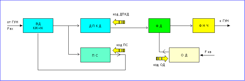
The block diagram of the synthesizer [1] is shown in Fig. 1, where the following designations are accepted:
The synthesizer control code is shown in Fig.2.
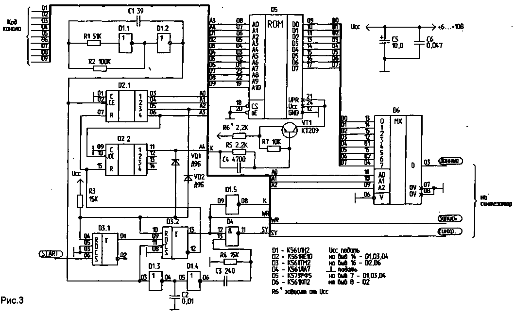
The main frequency ratios of the synthesizer: - dF - minimum frequency grid step; - dF=N*Fo, where N is an integer by which the division factor of the VD changes; - Fo - reference frequency of FD; - FBX - synthesized frequency Fin \uXNUMXd Fo * K * Kdpkd + Fo * N * Kps, where K is the division coefficient of the VD (Kvd). Calculation of the division coefficients whole number without remainder. The division coefficient of the PS Kps \uXNUMXd (Fin / (Fo * K) - Kdpkd) / (N * Fo), i.e. the remainder of the division when calculating the efficiency, divided by the minimum frequency grid step. Division coefficient OD Code = Fkv / Fo, i.e. the frequency of the reference crystal divided by the reference frequency of the PD. Some types of synthesizers have fixed OD division ratios (KR1015HKZ has Code=1024; 2560; 5120). Synthesizer calculation example 1. Initial data: - synthesizer - microcircuit KR1015HKZ (Kdpkd <4095, Code 5120, 2560,1024; Fmax<10 MHz). - external divider K1507IE1 (Kvd 10/11,20/22,40/44); - Fin= 135000 kHz; - dF=25kHz. 2. Based on Fin and Fmax, we select Kdel 20/22, i.e. Kvd=20, N=2. Next, we calculate Fo as dF/N=25/2= 12,5 kHz. Let's take Code=1024, then Fkv=12,5*1024=12800 kHz. If we take Kdel 40/44, we get Fo=6,25 kHz and with Code=1024 Fkv=6,25*1024=6400 kHz. Now let's define dFdpkd (frequency step per DPKD code unit) as FoKvd=b,25*40=250. Next, you can calculate the DPKD code and the PS code: Code DPKD=Fin/(dFdpkd==135000/250=540. Since the remainder is zero, code PS=0. For a frequency of 135050 kHz, the remainder = 50 and, therefore, the code PS=50/25=2. 3. When calculating, the following restrictions must be taken into account: - minimum and maximum DPKD codes (determined by the selected synthesizer type); - the maximum PS code must be > Kvd; - maximum frequencies for signal and reference oscillator inputs. Universal Synthesizer Control Circuit This version of the scheme is designed for the VHF FM band 145 MHz, 80 main and 80 additional channels. The scheme consists of two main (independent) nodes: - scheme for generating and entering the code of the synthesizer; - scheme for generating the channel number and indication. The circuit for generating and entering the code (Fig. 3) is designed for a synthesizer of the type KR1015XK3 or any other with code input in serial form (up to 32 bits). The given variant is designed for a twenty-digit code. To change the code capacity, it is necessary to change the K recalculation of the counter D2. Codes of frequencies entered into the synthesizer are recorded in ROM. How to compose a ROM firmware is described below.
The scheme includes the following nodes: - generator and counter-divider by 20 (D1.1, D1.2, D2, VD1, VD2); - launch and binding scheme (D3, D1.5); - scheme for generating code and recording signals of the synthesizer (D5, D6, D1.3, D1.4, D4, VT1). The circuit is started by the START pulse. The binding circuit generates a count enable pulse D2 and power on D5, tied to the leading edge of the generator pulses D1, D2. After counting 20 pulses, the trigger circuit returns to its original state and power is removed from D5. Data is output from the D6 output, data input clocks to the synthesizer are output from the D4 output, and a code write signal to the synthesizer PDCA is output from output 13 D3.2 (it can have a constantly high level). Operation of the universal synthesizer control circuit 1. The code of the selected channel is set (TTL levels at pins 1-6,23, 22,19D5). 2. The signal START (positive pulse) is set to "1" trigger D3.1. 3. The positive edge of the clock generated by the generator at D 1.1, D 1.2 is set to "1" trigger D3.2. A low-level signal from pin 12 D3.2 allows the counter (coefficient 20) to work on D2.1, D2.2, and a high-level signal from pin 13 D3.2 allows the output of clock recordings to the synthesizer through D4 and power is supplied to ROM D5 using D1.5 and VT1. A high-level signal is also formed at the synthesizer select input (REC). 4. The data entered into the synthesizer is converted into a serial code using the D6 multiplexer. 5. Data recording clock pulses are formed from generator pulses D1.1, D1.2 by elements D1.3, D1.4, C2, C3, R4. The clock pulse of the generator is delayed, and then a short pulse is formed from its leading edge. Thus, the write clock always exactly falls on the corresponding data bit. 6. After the counter counts 20 pulses, high-level signals appear on pins 11 D2.2 and 5 D2.1, which leads to the appearance of a high-level signal on pins 4 D3.1 and 10 D3.2. Triggers D3.1, D3.2 are set to their initial state. Thus, the counter stops counting, the power is removed from the ROM, the supply of the write clock to the synthesizer stops, the synthesizer selection signal (REC) goes low, and the entered data is entered into the synthesizer counters. 7. After changing the code, a START signal must be given, and the new code value is entered into the synthesizer. 8. The circuit is built on CMOS microcircuits that can be powered by a voltage of 3 ... 15 V. The ROM is powered by 5 V, and therefore the resistor R6 must be selected depending on the supply voltage so that when power is applied to the ROM, it does not exceed 5 .. .5,5 V 9. It should also be taken into account that the synthesizer usually has TTL levels for control inputs, so it may be necessary to turn on the level clamping circuits for the signals supplied to the synthesizer. Level fixing circuit - a resistor (1 ... 5 kOhm) connected in series to the signal circuit and a diode connected by the cathode to the synthesizer power circuit. 10. The above adjustment scheme does not require. The frequency of the generator is not critical, at the indicated ratings - about 100 kHz. The scheme for generating the channel number and indication The circuit (Fig. 4) contains a BCD counter of the channel number (D5, D6), which is used to indicate the channel number (D7, D8, HL1, HL2) and address the ROM. The maximum channel number that can be implemented in this scheme is 99 (in the above scheme, the maximum channel number is 80).
When the counter is turned on and overflowed, the circuit is set to the 40th channel (it can be set by any soldering of the inputs SO ... S3 of the counters D5, D6). Buttons S1, S2 increase or decrease the channel number. The S3 button is designed to modify the synthesizer code, for example, to reduce the transmission frequency by 600 kHz in repeater mode. On elements D1.5, D1.6, D2.6, D4, a counter installation scheme is made. On the elements C8...C11,VD4...VD7,R14...R18, a START signal generation circuit is made for the synthesizer code input circuit. As can be seen from the diagram, the START signal is generated in the following cases: - changing the channel number (by buttons S1, S2); - code modification (by pressing and releasing the S3 button); - when the power is turned on (elements D1.5.D1.6). START signal generation circuit Figure 5 shows a variant of the START signal generation circuit, which is convenient to use when using coding switches of the PP8-1 type or similar instead of the electronic circuit for generating the channel number. This circuit is, in fact, a circuit for linking the phase of the code writing pulse in the DPCD to the phase of the synthesizer reference frequency, which eliminates the appearance of mismatch pulses at the output of the synthesizer phase discriminator when writing a constant code in the DPCD.
Operation of the START signal generation circuit (Fig. 5) From the positive edge of the generator pulse, a short positive START pulse is formed, which is fed to the synthesizer control circuit. From the negative edge of the generator pulse, an impulse of setting to "1" of the trigger is formed. The positive edge of the reference frequency signal of the synthesizer (pin 14 KR1015HKZ) resets the trigger to "0". The signal (negative drop) from the output of the trigger enters the information entered into the synthesizer into its counters. Thus, the recording of information is time-bound to the reference frequency of the synthesizer, the appearance of mismatch pulses at the output of the phase detector of the synthesizer and the frequency stick-out in the PLL ring are excluded. The oscillator frequency should be selected based on the speed of the circuit's response to a channel change (1...10 Hz). It should be taken into account that the signal coming from the synthesizer has a high level - about 5 V. Therefore, the circuit operates at a supply voltage of no more than 9 V. Otherwise, a level clamping circuit must be installed at the output. The scheme is not critical to the ratings of the elements and does not require configuration. Author: S. Gurov, St. Petersburg; Publication: N. Bolshakov, rf.atnn.ru
Artificial leather for touch emulation
15.04.2024 Petgugu Global cat litter
15.04.2024 The attractiveness of caring men
14.04.2024
▪ Atomic clock on quantum entanglement ▪ Very early classes have a negative impact on student achievement ▪ Flying at 68 terabitometers per second ▪ NXP Solar Mobile Phone Solution ▪ Holding hands synchronizes brain waves and relieves pain
▪ section of the site Big encyclopedia for children and adults. Selection of articles ▪ article by Gabrielle Boner Chanel (Coco Chanel). Famous aphorisms ▪ article When did surfing originate? Detailed answer ▪ article Pharmacist-analyst. Job description
Home page | Library | Articles | Website map | Site Reviews
www.diagram.com.ua |


 Leave your comment on this article: