|
|


 Arabic
 Bengali
 Chinese
 English
 French
 German
 Hebrew
 Hindi
Hindi Italian
 Japanese
 Korean
 Malay
Malay Polish
 Portuguese
 Spanish
 Turkish
 Ukrainian
 Vietnamese
|
ENCYCLOPEDIA OF RADIO ELECTRONICS AND ELECTRICAL ENGINEERING Transceiver HDK-97. Encyclopedia of radio electronics and electrical engineering
Encyclopedia of radio electronics and electrical engineering / Civil radio communications In the proposed design, many nodes from other devices are used, the descriptions of which were published in amateur radio literature. This approach allowed the author of this article to create a relatively simple multi-band transceiver with good technical characteristics. Transceiver "HDK-97" is designed for ON and SSB communications on amateur bands 10, 15, 20, 40, 80 and 160 meters. During its development, the task was to create a technologically advanced and easily repeatable device using the already known (best, according to the author) amateur radio circuitry. Several copies of transceivers were manufactured with the following technical characteristics:
The transceiver is made according to the scheme with one frequency conversion and consists of 14 functionally completed blocks. The basis of the apparatus is block A1 (Fig. 1). This is a low-signal reverse transceiver path, the description of which was published in [1]. It has been subjected to some modifications. Without going into details, we only note that additions were made to the scheme, which made it possible to significantly improve the operation of the path.
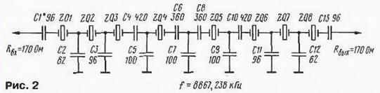
In the cascade control circuit on the transistor VT1, for example, relay K1 is introduced. With its contacts in the transmission mode, it disconnects the coupling coil of the transformer T1 from the target of the emitter of the transistor, preventing the self-excitation of the cascade. Automatic gain control is carried out at an intermediate frequency, and not at a low one, as it was in the original source. The source circuit of the resonant IF amplifier on the VT3 transistor includes an AGC control cascade on the VT4 transistor. In the absence of a signal (in receive mode), a voltage of about +3 V from block A1 (AGC) is supplied to pin 3,5 of block A5. Transistor VT4 is open and the IF has maximum gain. With the advent of the signal, the AGC voltage decreases from +3,5 V to zero, the VT4 transistor closes and, accordingly, the cascade gain on the VT3 transistor drops. The load resistance of the ZQ1 quartz filter (determined by the resistor R12) does not change, since the collector VT4 is connected at high frequency to a common wire through the capacitor C13. The second mixer on the T5VD20-VD23T6 is supplemented with a tuning resistor R16, which made it possible to balance the mixer and completely get rid of the carrier. Improved decoupling of the second mixer with UZCH cascades. At the IF frequency, it is constantly loaded with 50 ohms through the capacitor C24, and the L10C25 chain prevents it from being unbalanced by subsequent stages. The preliminary UZCH is made on two transistors - VT5 and VT6. It has a high gain with a low level of self-noise. The replacement of the DA1 (VLF) KV74УН4 chip with the К174УН7 chip made it possible to remove the problem of self-excitation of the amplifier and simplify this assembly (there was no need for a +9 V stabilizer). The use of the K140UD6 (DA2) chip in the microphone amplifier instead of transistors simplified the establishment of this cascade. The path is supplemented with a self-control device in the transmission mode (T7VD16-VD19), which is borrowed without changes from [2]. On fig. 2 shows a diagram of a quartz filter. It is made according to the ladder scheme on imported resonators used in TV decoders.
With good repeatability, the filter requires almost no tuning. Its main characteristics are as follows:
The GPA scheme (A2) is shown in fig. 3.
The master oscillator is made on an analogue of the lambda diode, which is assembled on transistors VT2 and VT3. Devices of this type have high efficiency, good temperature stability, relatively large and, most importantly, stable output signal amplitude. The master oscillator is powered by a stabilizer on the elements VT1 and DA1. Transistor VT4 - broadband buffer amplifier. Chip DD1 allows you to get the same amplitude RF voltage at the generator output over the entire frequency range. The generator is rebuilt with a double KPES11 in parallel with which additional capacitors are connected by relay contacts K1 - K5. In table. 1 shows the frequencies that the GPA covers when operating on different ranges, and the reference designations of the elements corresponding to them.
Relay K5 and capacitor C10 are introduced in case, when repeating the design, there is a desire to introduce an additional range. On the VD2 varicap, a detuning circuit is made, which is switched on by the contacts of the K6 relay. On fig. 4 shows the diagram of the GPA signal amplifier (block A3). This is a broadband amplifier with negative feedback. Such amplifiers have a low noise level, low frequency response unevenness, input and output impedances that are weakly dependent on frequency (close to 50 Ω), and a relatively large dynamic range [3].
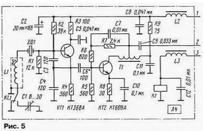
The A4 reference oscillator is made according to the capacitive three-ton scheme with quartz frequency stabilization. His diagram is in Fig. 5.
By adjusting the inductance of the coil L1, connected in series with the quartz resonator ZQ1, you can lower the frequency of the generator. Connecting capacitor C1 increases its frequency. This is how the working sideband is inverted. The AGC amplifier (block A5) is two-channel. Chip DA1 and diodes VD1 and VD2 (Fig. 6) track signals with a level of more than 9 points, and DA2 and VD5VD6 - signals with a level of 3 to 9 points. The node on the transistor VT1 allows you to adjust the discharge time of the capacitor C8 and avoid AGC "popping".
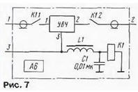
Block A6 - UHF receiving path. Its circuit is identical to that of the GPA amplifier and is therefore shown in Fig. 7 as a switchable module.
Block A7 - bandpass filters operating both for reception and transmission. The scheme and design of the block are completely borrowed from (4). Only the design and winding data of the contours have been changed, which will be discussed a little later. Block A8 (Fig. 8) includes an antenna switch (reception / transmission), a switchable attenuator of the receiving path and preliminary stages of the transmitter.
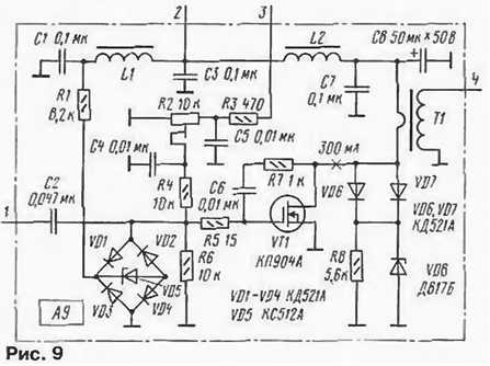
In the receive mode, the signal from the antenna through the normally closed contacts of the relay K1 is fed to the contacts of the relay K2 of the attenuator, which is assembled on resistors R1-R3. If necessary, the attenuator is turned on by applying voltage to the coil of relay K2. Further, the signal through the normally closed contacts of the relay K3 enters the block A7. In the transmission mode, the signal from block A7 through the contacts of relay K3 is fed to a broadband amplifier made on transistors VT1-VT3. Chains R4R6C2 and R21C15 correct the frequency response of the amplifier. The power amplifier circuit A9 (Fig. 9) is borrowed from [5] with virtually no changes.
The block diagram of the A7 bandpass filters (see the first part of the article) is shown in fig. 10.
The A10 low-pass filters (Fig. 11) and the A12 CW filter (Fig. 12) are borrowed from [5] almost unchanged.
The basis of the A11 CW generator (Fig. 13) was taken as a master oscillator circuit with a frequency shift from the A4 block.
The manipulation is carried out by closing the emitter of the transistor VT1 to a common wire through the R3R4C5C6 chain, which forms the front and fall of the telegraph message. The A13 power supply stabilizer and the RF voltage indicator in the A14 antenna have no special features. Their schemes are shown in Fig. 14 and 15 respectively.
The scheme of interblock connections of the transceiver and the purpose of the controls are shown in Fig.16.
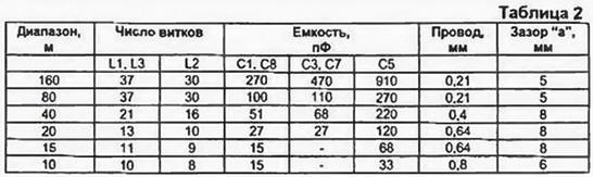
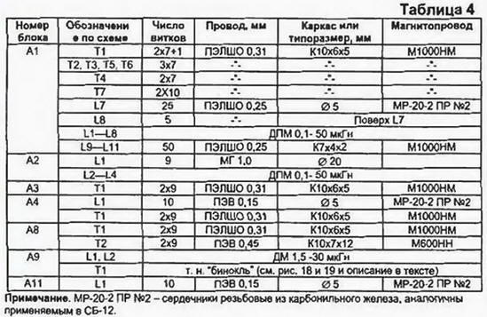
All transceiver blocks are made on printed circuit boards made of double-sided foil fiberglass. The transceiver uses widely used parts: fixed resistors such as MLT and C1-4, tuned - SPZ-19, SPZ-22, SP4-1. Adjusting resistors of the main controls (Fig. 15) - SP-1 and SPZ-12. Permanent capacitors of types KM, KLS, KD, K10-17v, oxide capacitors - K50-16, K50-35, K50-29. Capacitors of the master oscillator in block A2 (GPA) - type KSO or SGM (group G). Capacitor of variable capacity C11 - type KPE-2 (2x12 ... 495 pF), in which "two through one" rotor and stator plates are removed. Switches: SA1 - biscuit 11PZN, SA2 - SA8 - MTD1 microtoggle switches, SA9 - T1 toggle switch. Relay in blocks: A1-A2 - RES49 (passport RS4.569.425); A4, A7, A12 - RES49 (passport RS4. 569.423); A7 and K1, K2 in fig. 15 - RES47 (passport RF4.500.417). In block A8, relays K1 - RES47 (passport RF4.500.419), K2 - RES60 (passport RS4.569.438), K3 -RES55A (passport RS4.569.602). The winding data of the inductors of blocks A7 and A10 are given in Table. 2 and 3, respectively, the data of the coils and transformers of the remaining blocks are in Table. 4.
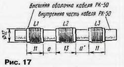
The GPA coil L1 is wound on a ceramic frame, pre-coated with a thin layer of BF-2 glue. After winding, the coil should be dried at a temperature of about + 100 ° C, placing it in an oven for one hour. The design of one of the coils of block A7 is shown in fig. 17.
As a frame, a piece of coaxial cable with an outer diameter of 12 mm was used, from which the central core and braid were removed. Moving the coils L1 and L3 with respect to L2 allows you to adjust the frequency response of the filter. On fig. 18 and 19 show the design of the power amplifier transformer T1.
Copper tubes located inside the ferrite magnetic circuits form the transformer winding in the drain circuit of the transistor. Secondary winding - two turns of MGTF 0,35 wire. Ferrite magnetic cores М600НН size K 10x7x12 mm. The transceiver power supply transformer is based on the standard TC-160. The secondary windings are removed from it, and new windings are wound in their place - 2x75 turns of wire PEV-21,5 (II-II`) and 2x2 turns of wire PEV-2 0,4 (III-III`). Sketches of the transceiver design are shown in fig. twenty.
At the first stage, the transceiver is tuned in the receive mode. and start it by checking the output voltages of the power supply at idle (the transceiver nodes are disabled). After making sure that it is in good condition and that the voltages indicated on the diagram are present, all blocks are connected, with the exception of +40 V circuits. In a smooth range generator, a tuning resistor R3 achieves stable operation of the master oscillator. Then, by selecting capacitors C4 - C10, the ranges are "stacked" according to Table. 1. Thermal compensation, if necessary, is carried out according to the method repeatedly described in amateur radio literature. By selecting a capacitor C16, the required detuning range of the generator is set, and by selecting a capacitor C12, a signal shape close to a meander is achieved at the outputs of the elements DD1.2 and DD1.3. When the transistor VT4 overheats, a resistor with a resistance of 100 ... 200 Ohms should be included in its source circuit. The trimmer resistor R8 sets the RF voltage at the output of the GPA amplifier (A3) within 1,5 ... 1,7 V. By selecting the capacitor C6 in the reference quartz oscillator (block A4), an output voltage of 0,7 ... 1 V is achieved. Then the frequency of the generator is "brought" to the lower slope of the characteristics of the quartz filter by adjusting the coil L1, and to the upper slope - by adjusting the capacitor C1. The setting of the main board A1 begins with setting the quiescent current of the transistor VT2 within 25 ... 30 mA by selecting the resistor R8. After that, by selecting the resistor R21, they make sure that the collector of the transistor VT6 has a voltage of +6 V. By disconnecting the input of the AGC unit from the main board, the voltage of +14 V is set at terminal 5 of the main board with a tuned resistor R3 of the A3,5 unit. By applying a signal with a GSS level of 1 ... 1 mV to output 10 of block A20 (any operating range) and adjusting the L7L8 circuit with the core, they achieve the maximum level of the low-frequency signal at the output of the transceiver. The quartz filter is matched by the selection of resistors R9 and R12. The resistance of the resistor R12 must be equal to Rin of the filter, and the resistance of the resistor R9 is 4Rin, since a 2:1 resistance transformer is included in the drain circuit of the transistor VT4 of block A1. If these conditions are not met, the frequency response of the filter will be distorted in the transmission mode. After that, it is necessary to restore the connection of the AGC input with the main board. The procedure for tuning bandpass filters is described in sufficient detail in [4]. Before setting up block A5, the IF gain control (resistor R2 in Fig. 16) is transferred to the lower position according to the diagram. With the trimmer resistor R15 of block A5, it is necessary to set the arrow of the PA1 device (S-meter) to the last division of the scale, and then move the IF gain control to the upper position. The engine of the tuned resistor R1 should be approximately 1/3 from the bottom position according to the diagram, and R8 should be in the middle position. Diode VD3 should be temporarily unsoldered. By applying a signal of 3 μV from the GSS to the input of the transceiver and adjusting the resistor R7, the deviation of the S-meter needle by 1 ... 3 scale divisions is achieved. If this fails, you need to increase the sensitivity of the node by adjusting the resistor R1. Before the next setup step, solder the VD3 diode in place, and unsolder the VD7 diode. By increasing the voltage of the signal from the GSS to the level of 50 μV, the trimmer resistor R4 sets the arrow of the device to the extreme right position. Next, the VD7 diode is soldered in place. By briefly applying a signal with a GSS level of 50 μV to the input of the transceiver, by adjusting the resistor R8, the AGC release delay time that is most comfortable for hearing is set. To adjust the output stages, the +40 V supply circuits are restored. An equivalent load of 1 Ohms with a power of 50 ... 25 W is connected to the XW30 antenna jack. At this stage, it is necessary to temporarily disconnect blocks A7 and A8. The transceiver is switched to transmission mode, and by selecting resistor R17 in block A8, a voltage of +3 V is set on the collector of transistor VT20. In power amplifier A9, by adjusting resistor R2, it should be ensured that the quiescent current of transistor VT1 is within 250 ... 300 mA. By pressing the telegraph key and adjusting the L1 coil of the CW generator (block A11), a signal with a frequency of about 1 kHz is set in the phones. After that, the connection between the DFT and the driver board is restored. The A7 low-pass filters are adjusted by shifting or expanding the turns of the coils of the corresponding ranges and selecting capacitors, focusing on the maximum readings of the RF voltage indicator (A 14) in the continuous CW signal transmission mode. In the event of a drop in transceiver power on the HF bands, it is necessary to select capacitor C9 in block A8. Setting up the transceiver is described here in a simplified way. More detailed recommendations can be found in [1 - 5] The transceiver uses the digital scale of V. Krinitsky, the description of which is given in the collection "The best designs of the 31st and 32nd exhibitions of the creativity of radio amateur designers" (Publishing house DOSAAF, 1989). Literature
Author: V.Gladkov (RW4HDK)
Machine for thinning flowers in gardens
02.05.2024 Advanced Infrared Microscope
02.05.2024 Air trap for insects
01.05.2024
▪ Huge unknown lake found under Antarctica ▪ Huawei NetEngine 9000 Petabit Backbone Router ▪ Headphones will match the music to your mood
▪ section of the site Wonders of nature. Article selection ▪ article Let the genie out of the bottle. Popular expression ▪ Article Providing first aid for fractures
Comments on the article: Arthur Thank you, a wonderful and useful article for those who want to build a reproducible apparatus! 73!
Home page | Library | Articles | Website map | Site Reviews
www.diagram.com.ua |


 Leave your comment on this article: