|
|


 Arabic
 Bengali
 Chinese
 English
 French
 German
 Hebrew
 Hindi
Hindi Italian
 Japanese
 Korean
 Malay
Malay Polish
 Portuguese
 Spanish
 Turkish
 Ukrainian
 Vietnamese
|
ENCYCLOPEDIA OF RADIO ELECTRONICS AND ELECTRICAL ENGINEERING K174XA42 - single-chip FM radio receiver. Encyclopedia of radio electronics and electrical engineering
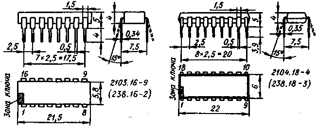
Encyclopedia of radio electronics and electrical engineering / radio reception Microcircuits K174XA42A and K174XA42B are designed to work in economical broadcasting and communication receivers of frequency-modulated signals. The microcircuits contain all the functional units of a superheterodyne FM receiver (from the antenna input to the AF output) and require a minimum of attachments for its implementation: a resonant LC circuit, several capacitors and one resistor. The adjustment of such a receiver comes down to setting the local oscillator circuit - setting the range limits. This became possible due to the low intermediate frequency - 70 kHz, which makes it possible to use non-tunable RC filters for signal selection, abandoning critical bandpass resonant LC filters. Large values of the input signal deviation - 50 and 75 kHz - at low IF lead to distortion of the AF signal. To eliminate them, a frequency feedback system was used, which reduces ("compresses") the deviation by a factor of five - up to 10 and 15 kHz, respectively. The microcircuit is equipped with a highly efficient noise suppression correlation system (noiseless tuning - BSN). It suppresses the audio signal during inaccurate tuning, near-noise input, and when tuned to an image channel. The K174XA42A device is designed to work in communication radio receivers. and K174XA42B - in broadcasting receivers for domestic purposes. The K174XA42 microcircuit can also be used in radio paths of television equipment, in telephones with a radio channel, in personal and business radio communication systems, paging devices, security devices, and telecontrol equipment. The small number of external elements required, ease of setup, and low cost make it highly attractive for widespread use in amateur radio designs. This microcircuit is produced in a plastic case in two versions: K174XA42A - in an eighteen-pin package 2104.18-4 (238.18-3), and K174XA42B - in a sixteen-pin package 2103.16-9 (238.16-2). The housing drawings are shown in fig. 1. The mass of the device does not exceed 2,5 g. The complete analogue of K174XA42A is the TDA7000 microcircuit; K174XA42B and TDA7010 differ only in case type.
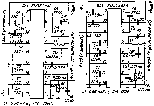
Typical circuits for switching on microcircuits K142XA42A and K174XA42B are shown in fig. 2a and b, respectively. Pinout K174XA42A: pin. 1 - connection of the correlator filter capacitor; pin. 2 - AF amplifier output (open collector); pin. 3 - connection of the noise generator capacitor; pin. 4 - connection of the OS loop filter capacitor by frequency; pin. 5 - positive power output; pin. 6 - connection of the LC circuit of the local oscillator; pin. 7-12 - connection of IF bandpass filter capacitors; pin. 13,14 - input of the radio frequency signal amplifier; pin. 15 - connection of the capacitor of the input circuit of the limiting amplifier 1; pin. 16 - general conclusion; negative power output: pin. 17 - connection of the capacitor of the phase shifter of the frequency detector; pin. 18-connection of the correlator phase shifter capacitor.
The K174XA42B chip, compared to the K174XA42A, has no pins 3 and 10, which is why the numbering of the pins in its pinout is accordingly shifted. Basic electrical characteristics at Tacr. cf ° 25±10°C Rated supply voltage, V....4,5
* These parameters are measured under the following conditions: supply voltage 4,5 V, RF input frequency 69 MHz, frequency deviation -+50 kHz, base frequency 1 kHz; when measuring the AM rejection ratio, the modulation depth is 30%. Maximum permissible values of parameters Supply voltage, V....2,7...9
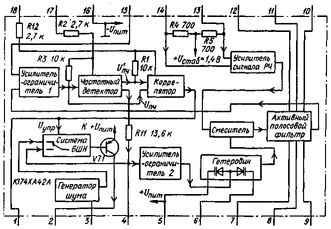
A simplified functional diagram of the K174XA42A device is shown in fig. 3. The FM receiver is built according to a superheterodyne scheme with a single frequency conversion. The input signal after amplification is mixed with the local oscillator signal. Due to the relatively low intermediate frequency (IF) of the signal taken from the mixer output, the amplitude of the conversion side components is so small that they are practically absent at the input of the intermediate frequency signal amplifier.
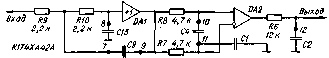
An active fourth-order IF filter is provided to suppress out-of-band signals. The output signal of the filter amplifier-limiter 1 normalizes the amplitude. Limiting amplifier 1 has a large gain (over 90 dB) and dynamic range. The converted IF signal is fed to the input of the frequency detector and simultaneously to the input of the correlator. The frequency detector is a frequency-voltage converter. The demodulated low-frequency voltage is supplied, firstly, to the second limiting amplifier and then to the local oscillator, closing the frequency feedback loop in the system, and, secondly, to the input of the switch of the noiseless tuning system (BSN) and then to the AF preamplifier and receiver output. The output signal of the correlator is used to control the switch of the BSHN system, which suppresses interoffice interference. In addition to these nodes, the microcircuit contains an internal supply voltage stabilizer (not shown in the diagram), an AF output amplifier (it is shown in the diagram as a transistor VT1) and a noise generator included in the BSHN system. The noise generator imitates FM noise and is connected by a switch to the input of the AF preamplifier when switching from one received station to another or when tuning is inaccurate. The noise signal in these cases indicates the operability of the receiving-amplifying path. The K174XA42B chip does not control the noise generator. The receiver uses frequency feedback demodulation - the output AF signal of the demodulator is used to appropriately offset the local oscillator frequency in antiphase with the IF signal. This achieved a decrease in the frequency deviation of the IF signal and, as a result, the almost complete absence of harmonic distortion of the output signal. The required degree of "deviation compression" is obtained if the capacitance of the oscillatory circuit of the local oscillator Co \u2d Sk + Cpar + Cvar is selected from the empirical relationship: Co \u1d Fo / 2 (Ck is the capacitance of the loop capacitor, Spar is the parasitic capacitance of the circuit, Cvar is the capacitance of the varicap - the tuning element , capacitance everywhere in picofarads; Fo is the loop tuning frequency, in megahertz). This expression, applicable for all frequencies in the VHF-XNUMX and VHF-XNUMX bands, allows you to determine the parameters of the local oscillator circuit - the capacitance of the capacitor, and then the inductance of the coil. The active band-pass filter of the IF microcircuit consists of three sections: a second-order high-pass filter, a first-order band-pass filter, and a first-order low-pass filter (see a fragment of the circuit in Fig. 4; the numbering of the capacitors corresponds to Fig. 2, a).
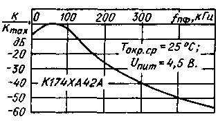
Bold dots indicate the pins of the microcircuit. The ratings of external capacitors and the values of the cutoff frequency of the links at an IF of 70 kHz are determined for the transfer function of the system according to the known relations [1]: LPF-II link: C9 = 3300 pF, C13 = 180 pF, fo = 94 kHz; link PF-I: C4 = 330 pF, C1 = 3300 pF, fv = 103 kHz, fn = 10,3 kHz; LPF-I link: C2 = 150 pF, fo = 88,4 kHz. The applied circuit design of the band-pass filter provides high selectivity, minimum power consumption and good dynamic range. The amplitude-frequency characteristic of the band-pass filter is shown in fig. 5.
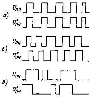
The BSHN system is used to suppress the signals of spurious reception channels. The operation of the system is based on the correlation of the IF signal and the same signal, delayed and inverted. Both signals are fed to the input of the correlator. If the direct signal Upf is a sequence of coherent pulses of a constant period (as is the case in the case of receiving a broadcasting station), then the signal delay U'f should be equal to the repetition period. Such a signal is obtained by inverting the direct signal. The signal is inverted and delayed by a phase filter (not shown in the diagram in Fig. 3). With fine tuning to the station, the shapes of both signals are identical and have a high degree of correlation (Fig. 6a). When detuned, the phase of the signal u'pch shifts relative to the straight line (Fig. 6,6) - the correlation is small. As a result of interference or noise, significant changes in the period and shape of the signal U'pch occur (Fig. 6, c); in these cases there is practically no correlation.
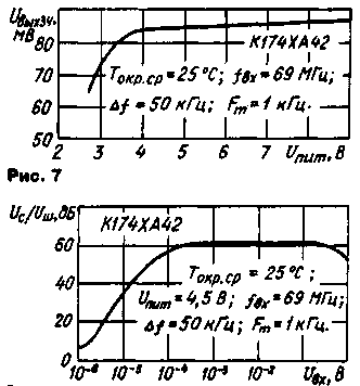
Based on the result of comparing these signals, the correlator generates a control signal for the switch, which smoothly turns on the AF amplifier at high correlation or the noise generator at low correlation. This eliminates the passage of various clicks, noise and harsh sounds to the receiver output. The exemplary voltage required for the operation of the frequency demodulator and correlator is formed by internal active phase shifters made on operational amplifiers with unity gain, the phase shifter (phase filter) provides a phase shift of the signal by n / 2 at a frequency fpch = K / Cf, where Cf is the capacitance capacitor connected to the pin. 17 microcircuits (see Fig. 3). With the resistance of the resistors R2 and R3 of the microcircuit indicated in this diagram, and the capacitance of the capacitor Cf equal to 330 pF (C7 in Fig. 2, a), fpch = 70 kHz. The input and output signals Upch and U'pch remain equal in voltage at any frequency. In the correlator, an internal phase shifter with an external capacitor connected to the pin. 18, shift the phase by another n/2. Thus, the total phase shift of the signals will be 180°. After inverting one of the signals, they are compared. The BSHN correlation system with frequency feedback ultimately provides a single receiving channel and fine tuning to a station. The output signal of the correlator (from pin 1) can be used to control the tuning indicator. Capacitor C16 (see Fig. 2a) determines the time constant of the silent tuning system. The R1C12 filter sets the time constant of the AF pre-distortion correction circuit. The level of noise entering the AF path depends on the capacitance of the capacitor C11; the larger the capacitance, the louder the noise. If it is necessary to ensure absolutely noiseless tuning, this capacitor is not connected. Capacitor C10 is part of the OS loop filter in frequency. It removes the IF spurious at the output of the frequency detector and determines the time constant of the feedback loop; also affects the shape of the amplitude-frequency characteristic of the path. Capacitor C15 is a filter in the power circuit of the microcircuit. Capacitor C5 turns the balanced RF input of the microcircuit into an unbalanced one. When mounting capacitor C5, it is necessary to shorten its terminals as much as possible and take measures to reduce the inductive and capacitive coupling with the local oscillator circuit. Capacitor C6 is a filter capacitor in the local feedback circuit of limiting amplifier 1, and C7 and C8 are phase-shifting capacitors of the phase filters of the frequency detector and correlator, respectively. Rice. Figure 7 illustrates the dependence of the AF output voltage Uoutp on the supply voltage Upit at fixed values of the input RF signal frequency fin, deviation and modulating frequency Fm and the nominal input voltage of the RF signal Uin.
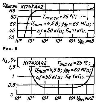
On fig. 8 shows the dependences of the output voltage of the AF, in fig. 9 - signal-to-noise ratios, and in fig. 10 - coefficient of harmonics from the voltage of the input RF signal.
Literature
Author: P.Polyatykin, Moscow; Publication: N. Bolshakov, rf.atnn.ru
Artificial leather for touch emulation
15.04.2024 Petgugu Global cat litter
15.04.2024 The attractiveness of caring men
14.04.2024
▪ Capacitors Panasonic SVT OS-CON ▪ Global warming affects the size of birds
▪ site section Electrical work. Article selection ▪ article Gradation of batteries by quality. video art ▪ What was France like in the XNUMXth-XNUMXth centuries? Detailed answer ▪ article The functional composition of Kitt TVs. Directory ▪ article Pseudo stereo mode on TV. Encyclopedia of radio electronics and electrical engineering
Home page | Library | Articles | Website map | Site Reviews
www.diagram.com.ua |

 Leave your comment on this article: