|
|


 Arabic
 Bengali
 Chinese
 English
 French
 German
 Hebrew
 Hindi
Hindi Italian
 Japanese
 Korean
 Malay
Malay Polish
 Portuguese
 Spanish
 Turkish
 Ukrainian
 Vietnamese
|
ENCYCLOPEDIA OF RADIO ELECTRONICS AND ELECTRICAL ENGINEERING Economical triac control device. Encyclopedia of radio electronics and electrical engineering
Encyclopedia of radio electronics and electrical engineering / Power Supplies The device is designed for compact and economical home automation products. It independently connects and disconnects one or more loads to the 220V AC mains, depending on an external logic signal. In this case, the pulse that controls the triac is formed with a minimum duration sufficient to open it [1]. In addition, the binding of the moments of switching on the load to the moments when the mains voltage passes through zero is provided, and the load always receives an integer number of periods of the mains voltage. This reduces the level of switching interference, which is especially important for high-power loads, and also guarantees the absence of a direct component of the load current.
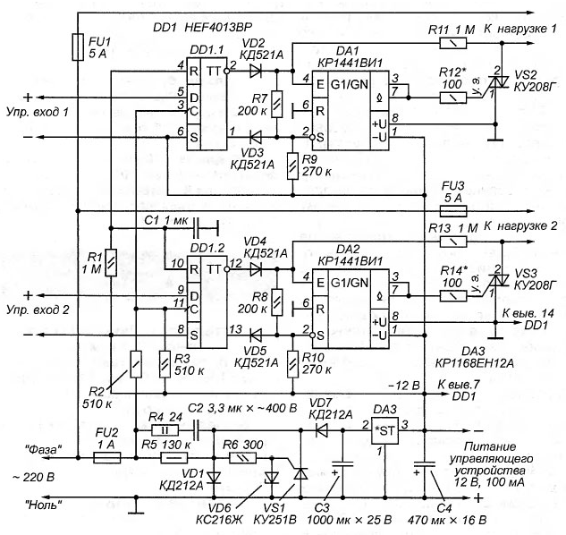
On fig. 1 shows a diagram of a device for independent control of two loads. Load 1 is switched by triac VS2. It is controlled by elements DD1.1, DA1, VD2, VD3, R7, R9, R11, R12. Similarly, load 2 is switched by triac VS3, which is controlled by elements DD1.2, DA2, VD4, VD5, R8, R10, R13, R14. So you can control any number of loads, while C1, R1-R3 are common to all. Elements R4-R6, C2-C4, VD1, VD6, VD7, VS1, DA3 form a power supply, the voltage of which is also supplied to an external control device. It provides an output voltage of 12 V at a load current of up to 100 mA. The block works on the principle of the power supply described in the article [2] with a ballast capacitor and an output voltage limiting unit on a zener diode and a transistor analogue of a trinistor. But instead of an analogue of the trinistor, a real device VS1 is used, as shown in Fig. 1. In my previous article [3], a triac control unit on the KR1441VI1 timer with a fixed duration of control pulses is described, and therefore its use in the case of load control with an inductive component is difficult. This article removes this limitation. The loads can be compact fluorescent ("energy saving") lamps with electronic ballast. If it turns out that the energy-saving lamp connected to the device flashes periodically in the off state, you need to try to select a triac with a lower leakage current, and if this fails, shunt the lamp with a resistor or capacitor, as recommended in article [4]. The triggers of the DD1 chip are used to synchronize the moments when the triacs are turned on with the mains voltage transitions through zero. Input D of each trigger is control - a signal is applied to it, which determines whether the corresponding load is turned on or off. The divider R2R3 provides the receipt of clock pulses to the inputs C of the triggers at the moments when the instantaneous voltage in the network passes through zero and grows (on the upper network wire relative to the lower one). Thus, the clock pulses follow at a frequency of 50 Hz synchronously with the network. At the moment the device is connected to the network, an impulse through the R1C1 circuit sets the device so that all loads are disconnected. Let's consider the operation of the device using the example of switching load 1. After turning on the power, the trigger DD1.1 is set to a high level state at the inverse output and a low level at the direct output. Here and below, the logic levels are indicated relative to the -12 V power line. This trigger is set to the same state when its input D (pin 5) is connected to the negative power wire after a clock pulse arrives at input C (pin 3). Diodes VD2 and VD3 open. A high level through diode VD2 is fed to input E (start enable signal - pin 4) of timer DA1, and a low level is set at its input S. As a result, the output of the timer DA1 (connected pins 3 and 7) is set to a high level. No current flows through the control electrode of the triac VS2, the triac is closed, load 1 is off. When connecting the input D of the trigger DD1.1 with a positive power wire after a clock pulse arrives at the input C, the trigger is set to a high level state at the direct output and a low level at the inverted output. Diodes VD2 and VD3 are closed. The state of the DA1 timer is determined by the voltage values at the outputs of the divider R11R7R9, which are connected to the inputs E and S of the timer. The resistances of the resistors of this divider are selected so that a current flows through the control electrode of the triac VS2 when the absolute value of the voltage U2-i between its electrodes 2 and 1 exceeds 9,8 V. The input E of the timer has a higher priority than S, and S has a higher priority than R. The input R of the timer is connected to the plus of its power supply. Therefore, the timer is in a low state at the output, if this is not prevented by the signals at the inputs E and S. As long as the absolute value of the voltage U2-1 is less than 9,8 V, a high level at the input E enables the setting of the input S. Input low level voltage S sets the timer to a high output state. No current flows through the control electrosimistor VS2, load 1 is disabled. If the voltage U2-i is greater than +9,8 V, then the voltage at the input S exceeds the switching threshold, so the signal from the input R switches the timer to a low state at the output. Current flows from the control electrode of the triac VS2 through the current-limiting resistor R12 to the timer output. Triac VS2 opens and connects load 1 to the network. If U2-1 is less than -9,8V, both E and S are driven low. A low input E switches the timer output low. Current flows from the control electrode of the triac VS2 through the current-limiting resistor R12 to the timer output. Triac VS2 opens and connects load 1 to the network. After opening the triac VS2, the voltage on it drops almost to zero, as a result of which the timer DA1, as described above, goes into a high state at the output, the current through the control electrode of the triac VS2 stops, resulting in economical control of the triac. If it is necessary that the load 1 is turned on after the input D of the trigger DD1.1 is connected to the negative power wire, and turned off - to the positive one, the connection of the inputs S and R, as well as the outputs of this trigger, is reversed. Resistors R12 and R14 set the current of the control electrodes of the triacs, which reaches 100 mA for the 100 Ohm resistance indicated in the diagram. This current is sufficient to open most triacs KU208G and all TS106-10-4. If the triacs used are selected so that they open with a current of 50 mA or foreign triacs MAC16D or BTA216-500V are installed, which are guaranteed to open with a current of 50 mA, then the resistance of resistors R12 and R14 can be increased to 200 ohms. Since the triac is controlled by a negative polarity voltage on the control electrode relative to its electrode 1 connected to a common wire, a negative polarity voltage is required to power the device. The proposed device can also be powered from the power supply of the control device, the output of which is connected to the capacitor C4, observing the polarity. In this case, the elements R4-R6, C2, C3, VD1, VD6, VD7, VS1, DA3 are not installed. In the absence of a noticeable inductive component in the load, the device consumes a current of about 200 ... 300 μA per load. However, for reliable starting, the power supply must provide at least 6 mA output current to the load. Be aware of the galvanic connection to the network and take precautions. The device must be placed in an isolated case and not connected directly to other devices, except those that it switches. To improve electrical safety, the network wire, which is common, is recommended to be connected to "zero", the other network wire to the "phase", as shown in the diagram.
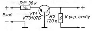
If the control device generates logic signals of positive polarity relative to the common wire, they are fed through a matching device, the circuit of which is shown in fig. 2. The resistance of the resistor R1 (in kiloohms) is calculated by the formula R1 = (Uvx1-0,7 V) / 0,1 mA, where UBX1 is the voltage of the high-level signal of positive polarity (in volts). In the denominator of the formula - the maximum rated current through this resistor is 0,1 mA. Indicated in fig. 2, its resistance corresponds to the high level of the TTL signal.
If the control device does not have its own power supply, then it can be powered from a bipolar power supply with a ballast capacitor, the circuit of which is shown in fig. 3. It is rated for output current up to 100mA per voltage. The control device is powered from the positive voltage, and the proposed one is powered from the negative voltage. It is undesirable to replace the HEF4013BP chip with analogues, since its counting inputs are equipped with Schmitt triggers. Nevertheless, it is possible to use other foreign microcircuits of the 4013B series. In extreme cases, K561TM2 can also be used, but then a Schottky diode KD3A, KD11A, KD7B or 923N922-922N1 (anode to pin 17) should be connected between pins 1, 19 and pin 7, which prevents current from flowing through internal protective diodes. Although this current does not exceed the value of 561 mA allowed for the K10 series, it leads to incorrect operation of the microcircuit. Timers KR1441VI1 can be replaced with similar imported ICM7555IPA, ILC555N, GLC555. It is also possible to use dual timers, such as GLC556, ICM7556IPD. An integrated stabilizer with an output voltage of -12 V (DA3 in Fig. 1 and DA2 in Fig. 3) can be from the KR1168EN12, KR1199EN12 series or imported type 79L12. The KR1170EN5 chip (DA1 in Fig. 3) is interchangeable with an analog 2931AZ-5. Transistor VT1 (see Fig. 2) - any of the KT3107 series. The MAC97A4 triac (VS1 in Fig. 3) can be replaced by the MAC97A6, MAC97A8, as well as any of the VT131 series. Trinistor VS1 (see Fig. 1) - any of the KU251, MCR100, VT149 series. Diodes VD1, VD7 in Fig. 1 and VD3, VD4 in Fig. 3 are from the KD105, 2D212, KD212 series (except for KD212B and KD212G), D237 (except for D237V, D237G and D237L), KD243, 1N4001 - 1 N4007. Diodes KD521A can be replaced by other low-power silicon ones. zener diode KS216Zh (VD6 in Fig. 1) can be replaced by 2S216Zh, KS508V, 1 N4703, BZX55-C16. The stabilization voltage of the zener diode used must be in the range of 15,5 ... 16,5 V at a current of 2 mA. Capacitors with a capacity of 3,3 microfarads with a rated voltage of 400 V (C2 in Fig. 1 and C1 in Fig. 3) are imported, marked "AC", intended for inclusion in an alternating current circuit. Literature
Author: K. Gavrilov
Machine for thinning flowers in gardens
02.05.2024 Advanced Infrared Microscope
02.05.2024 Air trap for insects
01.05.2024
▪ Production on TSMC 16FinFET Plus technology ▪ Dynamic heads using bamboo and opal analogue ▪ Children as a remedy for hypertension
▪ section of the site Stories from the life of radio amateurs. Selection of articles ▪ article Fireplace for bees. Tips for the home master ▪ article What is GBAS? Detailed answer ▪ article First aid for electric shock. Health care ▪ article Eating a glass. Focus Secret
Home page | Library | Articles | Website map | Site Reviews
www.diagram.com.ua |


 Leave your comment on this article: