|
|


 Arabic
 Bengali
 Chinese
 English
 French
 German
 Hebrew
 Hindi
Hindi Italian
 Japanese
 Korean
 Malay
Malay Polish
 Portuguese
 Spanish
 Turkish
 Ukrainian
 Vietnamese
|
ENCYCLOPEDIA OF RADIO ELECTRONICS AND ELECTRICAL ENGINEERING UPS laboratory power supply. Encyclopedia of radio electronics and electrical engineering
Encyclopedia of radio electronics and electrical engineering / Power Supplies In the article, the author tells how to make a laboratory power supply necessary in amateur radio practice from a faulty or outdated uninterruptible power supply. The main purpose of uninterruptible power supplies (UPS) is a short supply of various office equipment (primarily computers) in emergency situations when there is no mains voltage. The UPS consists of a battery (usually 12 V), a step-up voltage converter, and a control unit. In standby mode, the battery is recharged, in emergency mode, the voltage converter is turned on. Like all equipment, UPSs fail or become obsolete. Therefore, they can be used as a basis for the manufacture, for example, of a laboratory power supply unit (PSU). The most suitable for this may be UPS, in which voltage converters operate at low frequency (50 ... 60 Hz), and they include a powerful step-up transformer, which can also work as a step-down transformer. For the manufacture of a laboratory PSU, the KIN-325A UPS was used as a "donor". During development, the task was to obtain a simple scheme, while using as many elements from the "donor" as possible. In addition to the transformer and case, powerful field-effect transistors, rectifier diodes, a quad op-amp microcircuit, an electromagnetic relay, all LEDs, a varistor, some connectors, as well as oxide and ceramic capacitors were used. The power supply circuit is shown in fig. 1. The mains voltage through the fuse-link FU1 and the power switch SA1 is supplied to the primary winding of the transformer T1 (marking - RT-425B). The varistor RU1, connected in parallel with this winding, together with the fusible link protect the PSU from increased mains voltage. Through the current-limiting resistor R1 and the diode VD1, the HL1 LED is powered, indicating the presence of mains voltage.
A powerful rectifier on diode assemblies VD2-VD5 is connected to winding II (with a tap in the middle, rated voltage 16 V) of transformer T1. Depending on the position of the K1.1 relay contacts, the rectifier operates as a full-wave rectifier with a common transformer output (shown in Fig. 1) and an output voltage of about 10 V or as a bridge with an output voltage of about 20 V. The output voltage of this rectifier is supplied to the control element - field transistor VT1. Capacitors C1 and C3 smooth out the ripple of the rectified voltage, resistor R2 is a current sensor. Resistor R17 provides a minimum voltage regulator load in the absence of an external load. A low-power rectifier is assembled on diodes VD6-VD9 and smoothing capacitors C2 and C5. It is powered by a parallel voltage regulator on the DA1 chip, op-amp DA2, relay K1 and fan M1. The HL2 LED indicates the presence of voltage at the output of this rectifier. The adjustable voltage regulator is assembled on the op-amp DA2.3 and the transistor VT1. The exemplary voltage to the voltage regulator - resistor R11 - comes from the output of the stabilizer on the DA1 chip. The output voltage of the PSU from the trimmer resistor R12 is fed to the inverting input of the op amp DA2.3. This resistor sets the maximum output voltage. The adjustable current limiter is assembled on the op-amp DA2.1 and DA2.2. A voltage proportional to the output current from the sensor - resistor R2, is supplied to the voltage amplifier at the op-amp DA2.1 and then to the op-amp DA2.2, which compares it with the exemplary one supplied to its non-inverting input from the output of the resistive divider R4R7R8. Resistors R7 and R8 set the current limit threshold. Transistor VT2 controls relay K1. It will work when the voltage at the gate of this transistor exceeds the threshold value (for the transistor indicated on the diagram, the threshold voltage is 2 ... 4 V). The trimmer resistor R19 sets the output voltage of the PSU, above which the relay switches the output voltage of the rectifier. Transistor VT3 together with thermistor RK1 controls fan M1. It turns on when the temperature of the heat sink, on which the transistor VT1 and the thermistor are installed, exceeds a predetermined value. The threshold temperature is set by resistor R15. The supply voltage of the thermistor is stabilized by a parametric stabilizer VD11R16. The excess supply voltage of relay K1 drops across resistor R13, and fan M1 drops across resistor R18. If the load current does not exceed the threshold value, the voltage at the non-inverting input of the op-amp DA2.2 is greater than the voltage at the inverting one, at its output there is a voltage close to the supply voltage, so the VD10 diode is closed, and the current does not flow through the HL3 LED. In this case, the control voltage to the gate of the field-effect transistor VT1 comes from the output of the op-amp DA2.3 through the resistor R14 and the voltage regulator works. If the output voltage of the stabilizer is less than 4 V, the transistor VT2 is closed and relay K1 is de-energized. In this case, the voltage at the drain of transistor VT1 is 10 V. When the output voltage is more than 4 V, transistor VT2 opens and relay K1 is activated. As a result, the voltage at the drain of the transistor VT1 rises to 20 V. This technical solution improves the efficiency of the device. When the load current exceeds the threshold value, the voltage at the output of the op amp DA2.2 will decrease, the diode VD10 will open and the gate voltage of the transistor VT1 will decrease to a value that ensures the flow of the set current. In this mode, current flows through the HL3 LED, and it signals the transition to the current limiting mode. The limiting current is set by resistor R8 in the range of 0 ... 0,5 A and R7 - in the range of 0 ... 5 A. Capacitors C4 and C6 ensure the stability of the current limiter. Increasing their capacitance increases stability, but reduces the speed of the current limiter. The device uses fixed resistors - C2-23, R1-4 or imported, tuning - SP3-19, variables - SP4-1, SPO. In order for the scale of variable resistors that regulate voltage or current to be linear, they must be of group A. Thermistor - MMT-1. Resistor R2 is made from a piece of wire PEV-2 0,4 150 mm long. In addition to the function of a current sensor, it also works as a fuse in case of emergency. Oxide capacitors are imported, ceramic K10-17 can be used in place of non-polar ones. The fan is a computer fan with a consumption current of 100 ... 150 mA, its width must be equal to the width of the heat sink. Relay - any, designed for a switched current of 10 A and a rated voltage of the winding 12 ... 15 V. XS2, XS3 - sockets or terminal blocks. Most of the elements are placed on two printed circuit boards made of fiberglass laminated on one side with a thickness of 1,5 ... 2 mm. On the first one (Fig. 2), rectifiers are assembled, transistors VT2, VT3 are mounted with elements "surrounding" them, and some other details. The printed conductors connecting the elements of a powerful rectifier are "reinforced" - pieces of tinned copper wire with a diameter of 1 mm are soldered to them. The "regular" outputs of the T1 transformer are wired, they are equipped with two sockets. If you plan to use them, the plugs corresponding to them are mounted on the first board, which are soldered from the "native" UPS board.
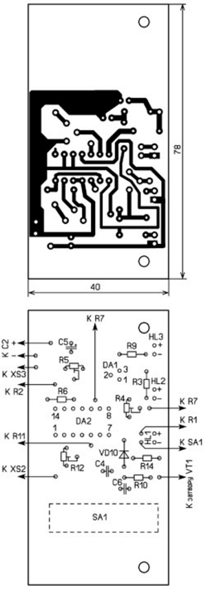
On the second board (Fig. 3) all microcircuits, LEDs, as well as some other elements are mounted. On the side free of printed conductors, a push-button switch SA1 (P2K or similar) is glued. The LEDs should go into the "regular" holes on the front wall of the case, a "regular" pusher is glued to the switch.
The first board is installed next to the rear wall of the case, the second - close to the front. To fasten the boards, two screws and "regular" fixing plastic racks on the top cover of the case were used. A ribbed heat sink with external dimensions of 30x60x90 mm (it is installed between the boards) houses a VT1 transistor, a thermistor and a fan. A heat-shrinkable tube is put on the thermistor and then glued to the heat sink next to the transistor. Since the field-effect transistor VT3 opens and closes smoothly when the temperature of the thermistor changes, the fan starts rotating and stops also smoothly. Therefore, the VT3 transistor can noticeably warm up and it is impossible to replace it with a low-power one, for example, 2N7000. On the front panel (Fig. 4), variable resistors and connectors XS2 and XS3 are installed in the holes, to which resistor R17 and capacitor C7 are soldered. Block plug XP1 and socket XS1 are "native", they are located on the rear wall in its lower part. The XS1 socket can be used to connect any device that works simultaneously with a laboratory PSU, such as an oscilloscope.
The adjustment begins with setting the maximum output voltage. This is done using the resistor R12, while the slider of the resistor R11 should be in the upper position according to the diagram. If it is not planned to build a voltmeter into the power supply, the resistor R11 is provided with a pen with a pointer and its scale is graduated. When transistor VT2 is open, by selecting resistor R13, the nominal voltage is set to relay K1, and when VT3 is open, resistor R18 is set to 12 V on fan M1. The fan switch-on temperature is set by resistor R15. To establish a current limiter, an ammeter and a load variable resistor with a resistance of 10 ... 15 Ohms and a power of 50 W are connected in series to the PSU output. The sliders of resistors R4 and R7 are set to the left position according to the diagram, the slider R8 is set to the right. The load resistor must have the maximum resistance. With an output voltage of about 10 V, a load resistor sets a current of 5 A, and a resistor R5 sets a voltage of 0,9 ... 1 V at the output of the op-amp DA2.1. With the help of a load resistor, the output load current is increased to 6 A and, by smoothly rotating the slider of the resistor R4, the HL3 LED is turned on (turning on the current limiting mode) and then the output current is set to 4 A by the resistor R5. When the slider of the resistor R7 is moved to the right (according to the circuit), the output current should drop to zero. In this case, resistor R8 can regulate the output current in the range of 0 ... 0,5 A. If you do not plan to build an ammeter into the power supply, the scales of these resistors are graduated. To do this (in the current limiting mode), the output voltage and load resistance are changed, the required current value is set, and marks are applied to the scale. In this case, in the range of 0 ... 0,5 A, the current is set by resistor R8 (resistor R7 must be in position "0"), and in the range of 0 ... 5 A - by resistor R7 (resistor R8 - in position "0") . In current limiting mode, batteries and rechargeable batteries can be charged. To do this, set the final voltage and charging current, and then connect the battery (accumulator). Further improvement of the proposed power supply is the installation of a built-in digital voltmeter, ammeter or combined measuring device. Author: I. Nechaev
Machine for thinning flowers in gardens
02.05.2024 Advanced Infrared Microscope
02.05.2024 Air trap for insects
01.05.2024
▪ Ball lightning - maybe it's just an illusion ▪ The influence of music on the state of memory ▪ Want to lose weight - sniff vanilla
▪ section of the site The most important scientific discoveries. Article selection ▪ article Shine and poverty. Popular expression ▪ article What is the greenhouse effect and how does it affect the Earth's climate? Detailed answer ▪ article by Joster Pursha. Legends, cultivation, methods of application ▪ article Pulse voltmeter. Encyclopedia of radio electronics and electrical engineering ▪ article Fuel flow meter for a car. Encyclopedia of radio electronics and electrical engineering
Home page | Library | Articles | Website map | Site Reviews
www.diagram.com.ua |


 Leave your comment on this article: