Voltage regulator on a CMOS chip. Encyclopedia of radio electronics and electrical engineering

Encyclopedia of radio electronics and electrical engineering / Surge Protectors
 Comments on the article
Power sources in which power elements operate in a key mode are more complicated than lithium sources with elements operating in an active mode, but their efficiency is twice or even three times higher than the efficiency of the latter. The efficiency of switching voltage regulators is high, since transistors in the closed and saturated states dissipate little power. In addition, the output does not require filters with large values of inductance and capacitance, since the ripple frequency is high (25...50 kHz). A switching voltage regulator with a constant switching frequency of the key element, but with a variable duration of its open state (PWM), is simpler than other types of stabilizers, and allows the use of low-frequency transistors.
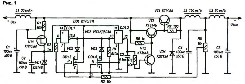
The proposed switching voltage regulator with PWM (Fig. 1) contains a pulse-width modulator made on a K176LP1 CMOS chip [1]. This is a multi-purpose chip containing a set of CMOS transistors (three p- and three n-channel). Inverters DD1.1 and DD1.2. each of which is formed by two transistors placed in the K176LP1 chip, together with a resistor R4 and a capacitor C3 form a multivibrator. The other two transistors of the K176LP1 chip (n-channel and p-channel) are connected in parallel to the output of the inverter DD1 1 and resistor R4.

(click to enlarge)
At a high level at the output of DD1.1, the diode VD2 is open, and, neglecting its resistance, we can assume that the p-channel of the transistor is connected in parallel with the resistor R4, and the channel resistance decreases with decreasing control voltage. Similarly, the n-channel is connected in parallel with the resistor R4 at a low level at the output of the inverter DD1.1 and open VD3 (the resistance of this channel decreases with increasing control voltage). Since, at any value of the control voltage, the output resistance of one field-effect transistor increases and the other decreases, the average value of the resistance shunting resistor R4 over the period is constant, and the generator oscillation frequency is also constant, i.e. only the duty cycle changes (from 1 to 99% of the period of the operating frequency), and it is directly proportional to the amplitude of the control voltage.
A sequence of pulses modulated in duration is fed from the output of the pulse-width modulator to the base of the transistor VT2, which unlocks and locks the key transistor VT4. Diode VD4 provides a closed circuit for the current of the inductor L2 when the transistor VT4 is turned off.
The stabilizer, by changing the duty cycle of the output pulses, allows a change in the output voltage over a wide range. However, since the output voltage has a double noise level, filters are included at its input and output (chokes L1 and L3, capacitors C1, C4, C5).
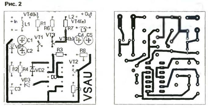
The voltage stabilizer works as follows. Part of the output voltage taken from the potentiometer R8 controls the duty cycle of the pulses generated by the pulse-width modulator, i.e. the ratio between the durations of the open and closed states of the key transistor VT4. When the voltage at the output of the stabilizer decreases, the control voltage taken from R8 decreases. as a result, the key transistor VT4 is open longer, and the powerful diode VC4 is closed, and vice versa, with an increase in the output voltage, the key transistor VT4 is closed longer, and the powerful diode VD4 is open. As soon as the key transistor VT4 closes, the VD4 diode immediately opens. and the energy stored in the inductor L2 is given to the load. The output voltage is set by potentiometer R8. The stabilizer is placed on a 52x52 mm printed circuit board made of double-sided fiberglass. The drawing of the board is shown in fig. 2.
In the stabilizer, instead of the KT908A transistor, you can use other powerful high-frequency transistors, for example, KT903A. or powerful low-frequency ones - KT803, KT805, KT808 At high load currents, the key transistor VT4 must be installed on a radiator to eliminate its overheating. As a VD4 diode, you can use a KD212 diode or a collector junction of a powerful high-frequency transistor. Inductors L1 and L3 are wound on pieces of a ferrite (600MN) rod 20 mm long and 8 mm in diameter. They contain 10 turns of wire PEV-2 01,2 mm. The inductor L2 is made on an armored ferrite (B26) core 2000MN with a gap between the cups of 0,2 mm. The L2 windings of the inductor are made of three PEV-2 00,2 mm wires twisted with a drill. The winding goes until the armor core is filled.
Literature
- M.E. Anglin. C-MOS 1C forms pulsewkrth modulator. - Electronics, 1977. vol 50. No. 13, P126.
- Seleznev V. Voltage stabilizer on the comparator. - Radio. No. 3. pp. 46-47.
Authors: V.Kalashnik, M.Eremin, R.Panov, Voronezh.
 See other articles Section Surge Protectors.
Read and write useful comments on this article.
<< Back
 Latest news of science and technology, new electronics:
Artificial leather for touch emulation
15.04.2024
In a modern technology world where distance is becoming increasingly commonplace, maintaining connection and a sense of closeness is important. Recent developments in artificial skin by German scientists from Saarland University represent a new era in virtual interactions. German researchers from Saarland University have developed ultra-thin films that can transmit the sensation of touch over a distance. This cutting-edge technology provides new opportunities for virtual communication, especially for those who find themselves far from their loved ones. The ultra-thin films developed by the researchers, just 50 micrometers thick, can be integrated into textiles and worn like a second skin. These films act as sensors that recognize tactile signals from mom or dad, and as actuators that transmit these movements to the baby. Parents' touch to the fabric activates sensors that react to pressure and deform the ultra-thin film. This ... >>
Petgugu Global cat litter
15.04.2024
Taking care of pets can often be a challenge, especially when it comes to keeping your home clean. A new interesting solution from the Petgugu Global startup has been presented, which will make life easier for cat owners and help them keep their home perfectly clean and tidy. Startup Petgugu Global has unveiled a unique cat toilet that can automatically flush feces, keeping your home clean and fresh. This innovative device is equipped with various smart sensors that monitor your pet's toilet activity and activate to automatically clean after use. The device connects to the sewer system and ensures efficient waste removal without the need for intervention from the owner. Additionally, the toilet has a large flushable storage capacity, making it ideal for multi-cat households. The Petgugu cat litter bowl is designed for use with water-soluble litters and offers a range of additional ... >>
The attractiveness of caring men
14.04.2024
The stereotype that women prefer "bad boys" has long been widespread. However, recent research conducted by British scientists from Monash University offers a new perspective on this issue. They looked at how women responded to men's emotional responsibility and willingness to help others. The study's findings could change our understanding of what makes men attractive to women. A study conducted by scientists from Monash University leads to new findings about men's attractiveness to women. In the experiment, women were shown photographs of men with brief stories about their behavior in various situations, including their reaction to an encounter with a homeless person. Some of the men ignored the homeless man, while others helped him, such as buying him food. A study found that men who showed empathy and kindness were more attractive to women compared to men who showed empathy and kindness. ... >>
| Random news from the Archive Vulnerability of Empires
18.12.2023
Scientists from the universities of Wageningen (Netherlands), Cambridge, Exeter (UK) and Washington State (USA) conducted a study on the question of the existence of patterns in the dynamics of the destruction of empires or societies. The study's findings, published in the journal PNAS, point to the importance of domestic factors in the context of states' vulnerability to collapse.
Domestic political processes play a key role in states' vulnerability to collapse. Understanding these patterns can help develop more effective strategies for managing and preventing potential crises in modern societies.
Professor Tim Kohler from the University of Washington, one of the authors of the study, emphasized that despite the influence of external factors such as natural disasters, their role is usually a trigger that activates the internal dynamics of the state.
Scientists analyzed the history of 324 ancient states, spanning five millennia. This approach, usually used to study the risk of death in aging people, was used for the first time to study the probability of the collapse of societies. The results showed that the risk of state collapse increases sharply in the first two centuries after their formation, after which it stabilizes. This allows some societies to last much longer than others.
This pattern has been identified both in the history of European societies of the modern era, and in the early civilizations of North and South America, as well as in the Chinese dynasties. For example, the ancient dynasties of China had a life expectancy limit of about 300 years over two millennia.
Researchers believe that despite significant differences between modern and ancient societies, the former may be subject to the same mechanisms that have influenced states for millennia. The social injustice, scarcity and extreme climate challenges that destabilized ancient societies can still cause discontent and violence in modern times.
|
Other interesting news:
▪ Mean Well PSC-160 Security Power Supplies
▪ Total Surveillance in New York
▪ Electric explosion of aluminum foil will effectively bond the metal
▪ Luminous Carpet - a smart guide in space
▪ Brain implants to restore vision
News feed of science and technology, new electronics
 Interesting materials of the Free Technical Library:
▪ website section Television. Article selection
▪ article If a friend turned up suddenly. Popular expression
▪ article What color were the real Oompa-Loompas? Detailed answer
▪ article Storekeeper. Job description
▪ article Keychain of emotional attunement. Encyclopedia of radio electronics and electrical engineering
▪ article Field effect transistors KP951 - KP973. Encyclopedia of radio electronics and electrical engineering
Leave your comment on this article:
 All languages of this page
Home page | Library | Articles | Website map | Site Reviews

www.diagram.com.ua
2000-2024


 Arabic
 Bengali
 Chinese
 English
 French
 German
 Hebrew
 Hindi
Hindi Italian
 Japanese
 Korean
 Malay
Malay Polish
 Portuguese
 Spanish
 Turkish
 Ukrainian
 Vietnamese