|
|


 Arabic
 Bengali
 Chinese
 English
 French
 German
 Hebrew
 Hindi
Hindi Italian
 Japanese
 Korean
 Malay
Malay Polish
 Portuguese
 Spanish
 Turkish
 Ukrainian
 Vietnamese
|
ENCYCLOPEDIA OF RADIO ELECTRONICS AND ELECTRICAL ENGINEERING Laboratory power supply 5...100 volts, 200 milliamps
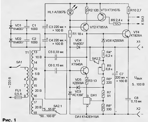
Encyclopedia of radio electronics and electrical engineering / Power Supplies In the practice of a radio amateur, from time to time there is a need for a stabilized constant voltage that exceeds the traditional 5 ... 15 V used to power equipment on microcircuits. In such cases, the described device will help. Source Specifications
High stability is ensured by the use of the KR142EN19A chip as a source of exemplary voltage and an amplifier of the mismatch signal [1]. The power supply circuit is shown in fig. 1. Its rectifier is assembled according to the scheme with doubling the voltage on diodes VD1 and VD2, which are shunted by capacitors C1 and C2 to reduce the level of switching noise. To reduce the power dissipated by the stabilizer transistors, when operating in the range of 5 ... 55 V, a part of the secondary winding of the transformer T1 is turned off by the SA2 switch.
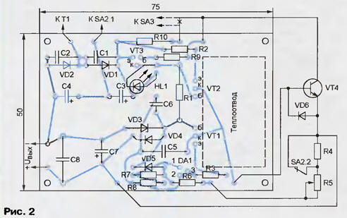
Transistor VT2 serves as a current generator. The voltage at its base is stabilized by the HL1 LED, the collector current value (8 ... 9 mA) is set by the resistor R2. Through a divider of resistors R4-R8, part of the output voltage of the stabilizer is fed to the control input of the DA1 microcircuit. If the voltage here is less than 2,5 V, the anode current of the microcircuit and the collector current of the transistor VT1 do not exceed 0,4 mA. Thanks to this transistor, connected according to a common base circuit, the voltage at the anode of the DA1 microcircuit does not exceed 3,3 V, and the power dissipated by it does not go beyond the permissible value. In this mode, almost the entire collector current of the transistor VT2 enters the base of the transistor VT4, opening the latter. The voltage at the output of the stabilizer and at the control input of the DA1 chip is growing. When the latter reaches 2,5 V, the anode current DA1, and with it the collector current of the transistor VT1, will increase sharply, the base current of the transistor VT4 will decrease and the voltage at the source output will be stabilized at a level determined by the ratio of the resistances of the resistors R4-R8. The output voltage is smoothly regulated by a variable resistor R5, the adjustment interval is selected using switch SA2. Transistor VT3 is normally closed. But with an increase in the load current and collector current of the transistor VT4 to about 250 mA, the voltage drop across the resistor R10 reaches a value at which the transistor VT3 opens, shunting the HL1 LED. This leads to a decrease in the collector currents of transistors VT2 and VT4. As a result, the output current of the stabilizer is limited to the above value. The operation of the current limiter can be judged by a decrease in the brightness of the LED. When, as a result of the action of the limiter, the voltage at the output of the stabilizer drops to approximately 2,7 V, the current flowing through the HL1R1 circuit will go to the load through the opened VD4 diode, slightly increasing the total current flowing through it. If there were no VD4 diode, as a result of a change in the polarity of the applied voltage, the collector junction of the transistor VT1 would open and the current flowing through R1 would go to the base of the transistor VT4. As a result of amplification by the transistor VT4, the load current increment would be much larger. It is possible to completely eliminate the effect of increasing current using a diode included in the open circuit connecting the collector of the transistor VT1 to the base of the transistor VT4 and the collector of the transistor VT2. But in this case, transistors VT1 and VT2 cannot be installed on a common heat sink without insulating gaskets. You should talk about the purpose of the diodes VD5 and VD6. Suppose the switch SA2 is in the "50 ... 100 V" position, and the minimum voltage is set at the output (the variable resistor R5 slider is in the upper position according to the diagram). After switching the switch SA2 to the "5 ... 55 V" position, a voltage of 50 V, to which the capacitor C7 is charged, is applied to the resistors R6-R9, moreover, more than half of it (about 30 V) to the control input of the DA1 microcircuit. The latter will not fail, but through the internal circuits of the microcircuit, this voltage will fall on its anode and on the emitter of the transistor VT1, closing the latter. As a result, the entire collector current of the transistor VT2 will flow into the base of the transistor VT4 and the maximum possible voltage will appear at the output of the stabilizer. Unfortunately, this state is stable and the stabilizer will not be able to get out of it on its own. Diode VD5 serves to eliminate such a critical situation. Opening, it limits the voltage at the input of the DA1 chip to an acceptable value. The correct choice of the stabilization voltage of the zener diode VD3 and the values of the resistors R7 and R8 ensures that in normal operating mode the VD5 diode remains closed and does not affect the operation of the stabilizer. With a sharp change in the position of the controls in the direction of decreasing the output voltage, a situation is possible when, due to the slow discharge of the capacitor C7, the voltage at the emitter of the transistor VT4 "does not keep up" with the voltage at its base. There is a danger of breakdown of the emitter junction of the transistor by a voltage applied to it in the opposite direction. Diode VD6 prevents this reversible but unwanted breakdown. Capacitor C7 is discharged through the circuit VD6, VT1, R3, DA1. Thanks to the resistor R3, the discharge current does not exceed 100 mA. The power supply unit uses a unified transformer TPP271-127/220-50 [2] with an overall power of 60 W. Such transformers of lower power have too large active winding resistances to work in the proposed device. To reduce the voltage on the secondary windings of the transformer, the outputs of its primary windings are connected in a non-standard way. When making the transformer yourself, you should be guided by those indicated in Fig. 1 no-load voltage of the secondary windings. The sections of the winding wires must be large enough so that the winding resistances are approximately the same as those of the specified transformer: 1-9 - 56 ohms, 13-16 -2,3 ohms, 17-18 -1,3 ohms. All fixed resistors in the device are C2-23 or MLT of the corresponding power, R5 is PPP-40. Capacitors C1 and C2 are ceramic for a voltage of at least 160 V, for example, KM-5 of the TKE group is no worse than M1500. C3, C4, C7 - imported analogues of K50-35, C6 - KM-5 or KM-6, C5 and C8 - K73-17 for a voltage of 250 V. Diodes 1N4007 have a domestic analogue - KD243Zh, you can use any diodes for a voltage of at least 200 V and current 300 mA. Instead of KD509A, you can install any diodes with a permissible pulse current of at least 300 mA. The current transfer coefficients h21e for all powerful transistors must be at least 30, and this parameter of the VT4 transistor should be checked at a collector current of 200 mA. Replacement transistors VT1, VT2 and VT4 must be selected with a maximum collector-emitter voltage of at least 160 V and an allowable collector current of at least 100 mA (VT1 and VT2) and 1 A (VT4). Transistor VT3 - any low-power silicon pnp structure. LED HL1 - any visible glow. To keep the collector current of the transistor VT2 unchanged when the HL1 LED is green or yellow, you may have to slightly increase the value of the resistor R2. The KR142EN19A chip can be replaced with an imported analog TL431. The main part of the power supply parts is placed on a 50x75 mm printed circuit board made of fiberglass 1,5 mm thick (Fig. 2, view from the side of the printed conductors). It also contains a common ribbed heat sink for transistors VT1 and VT2 with dimensions of 20x24x38 mm. The VT4 transistor is installed on a separate ribbed heat sink with dimensions of 36x100x140 mm. The VD6 diode is soldered directly to the terminals of this transistor.
It is advisable to connect the assembled device to the network for the first time through a laboratory adjustable autotransformer, at the output of which zero voltage is preliminarily set. The slider of the variable resistor R5 must be in the position of minimum resistance, the switch SA2 - in the "5 ... 55 V" position. A voltmeter is connected to the source output and they make sure that as the autotransformer handle rotates in the direction of increasing voltage, the voltmeter readings grow, but, having reached approximately 5 V, remain at this level. If so, you can bring the input voltage to the nominal 220 V and check the voltage on some elements of the device. At the cathode of the zener diode VD3, it should be close to its stabilization voltage (3,9 V), at the top terminal of the resistor R7 according to the circuit, it should be approximately 3,3 V. The voltage drop across the resistor R2 should be about 1,1 V, if it is greater, it is necessary to increase the value of the specified resistor so that the current flowing through it is within 8 ... 9 mA. Resistors R4, R6, R8 are selected in the following order. With the SA2 switch in the "5 ... 55 V" position, the maximum voltage at the source output is set using the variable resistor R5. The resistor R8 is selected so that it is slightly more than 55 V. The slider of the resistor R5 is moved to another extreme position and, by selecting the resistor R6, the output voltage is slightly less than 5 V. Then switch SA2 is set to the position "50 ... 100 V" and select resistor R4, achieving the specified limits for adjusting the output voltage by resistor R5. Be sure to check the operation of the power supply with the maximum load. If, in any range at maximum output voltage, an increase in load current leads to a decrease in this voltage, the point is insufficient voltage on the corresponding secondary winding or too high resistance of the windings. A milliammeter to control the output current can be included in the break of the wire going from the emitter of the transistor VT4 to other circuit elements (except for the VD6 diode). Since in this case, in addition to the load current, the divider current R4-R8 will also flow through the device, the milliammeter needle should be set to zero with the adjusting screw when the source is on, but operating without load. The device can be supplemented with a switch for the level of output current limitation (Fig. 3). The resistance of the introduced part of the circuit of resistors R10-R13 must be such that, at the current limit, a voltage of about 0,6 V drops across it.
It is easy to calculate the voltage stabilizer according to the above diagram for any adjustment interval of the output voltage with an upper limit of 50 ... 500 V. Transistors (except VT3) should be selected with approximately one and a half times the voltage margin relative to the maximum output. The current generator on the transistor VT1 should produce a current approximately 1,2 times the maximum output current of the stabilizer, divided by the coefficient h21e of the transistor VT4. With a rated output current of more than 1 A, a composite transistor is required as VT4. Currents through resistor R1 and divider R4-R8 can be selected within 4...10 mA. If the stabilizer is designed for a fixed or narrowly adjustable output voltage, diodes VD4 and VD6 can be omitted. Literature
Author: S. Biryukov, Moscow
Machine for thinning flowers in gardens
02.05.2024 Advanced Infrared Microscope
02.05.2024 Air trap for insects
01.05.2024
▪ Growing tomatoes in air-conditioned greenhouses ▪ Super Sub Electric Submarine
▪ section of the site Alternative energy sources. Article selection ▪ article Stolypin's tie. Popular expression ▪ article How was vulcanization discovered? Detailed answer ▪ article Accident on the water. Health care ▪ article Device for testing capacitors. Encyclopedia of radio electronics and electrical engineering ▪ Article Vanishing Warrior. Focus Secret
Home page | Library | Articles | Website map | Site Reviews
www.diagram.com.ua |


 Leave your comment on this article: