|
|


 Arabic
 Bengali
 Chinese
 English
 French
 German
 Hebrew
 Hindi
Hindi Italian
 Japanese
 Korean
 Malay
Malay Polish
 Portuguese
 Spanish
 Turkish
 Ukrainian
 Vietnamese
|
ENCYCLOPEDIA OF RADIO ELECTRONICS AND ELECTRICAL ENGINEERING Laboratory power supply, 220/0-20 volts
Encyclopedia of radio electronics and electrical engineering / Power Supplies The relative complexity of the proposed device is compensated by improved (compared to similar devices) parameters and consumer qualities. The author's recommendations allow both to simplify the design if desired, and to introduce additional functions into it. Compared with similar devices already described in the Radio magazine, the proposed power supply, in my opinion, has several advantages: firstly, unlike the previously proposed options for controlling the KP142EHJ2A integrated circuit, the voltage regulator is covered by the general purpose of feedback; secondly, the load current measuring resistor is connected directly at the output of the device, so the current actually consumed by the load is measured. In addition, the power supply does not contain manual output voltage limit switches. Instead, it has an automatic trinistor switch that switches the secondary windings of the transformer depending on the output voltage. Thus, the power dissipated by the regulating element of the stabilizer is reduced at low output voltages or during overcurrent. The power supply contains an LED indicator of the operating mode, which allows you to clearly fix the moment of transition from the voltage stabilization mode to the current stabilization mode, and vice versa. And finally, it does not require a selection of elements to accurately set the zero output voltage. Its scheme is shown in Fig. 1.
The device contains a unit for measuring the output voltage on the DA7 chip. adjustable voltage regulator (DA5. DA6). current limiting unit (DA2), indication unit (DA3), transformer winding switching unit (DA8.VS1) and auxiliary power supply (DA1, DA4). The network transformer T1 has three secondary windings, two of which (II and II ') are used to power the load and generate a voltage of +24 V to power the stabilizer, and the third (III) to obtain a voltage of -6 V. Rectifier diode bridges VD5-VD8 and VD1 - VD4 are connected in series, therefore, a voltage of about 13 V acts at the output of the first of them. and 26 V at the output of the second. From the output of one of the bridges, the voltage is supplied through the diode VD9 or the trinistor VS1 to the smoothing capacitors C6 and C7, and then - on the integral stabilizer DA5. The control voltage at pin 17 of this microcircuit is formed by the op-amp DA6 and the current amplifier on the transistor VT4. The voltage from the variable resistor R8 is applied to the non-inverting input of the op-amp. which set the desired output voltage. The inverting input receives a signal from a differential amplifier made on the op-amp DA7. This amplifier generates a voltage proportional to the output. The need for such a node is dictated by the fact. that a measuring resistor R20 of small resistance is connected in series with the load. The transfer coefficient of the amplifier is 0,33, so the voltage at its output is in the range of 0 ... 6,6 V when the output voltage of the source changes from 0 to 20 V. Op-amp DA6 generates such a signal that the difference in voltage values at its inputs is zero. Thus, the output voltage is stabilized. Capacitor C17 eliminates the self-excitation of the op-amp. The voltage across the resistor R20 is compared with the voltage taken from the divider R4-R6. If the voltage across the resistor R20 is less than that on the engine of the variable resistor R5, the output of the comparator DA2 is about 23 V. The VD11 diode is closed at this time. As soon as the load current reaches the limit set by the resistor R5, the voltage at the output of the op-amp DA2 will decrease, which will lead to the opening of the VD11 diode and a decrease in the voltage across the resistor R8. Thus, the "task" of the voltage stabilizer is changed, and its output voltage is reduced to a level at which the load current is equal to the limiting current. Self-excitation of the op-amp DA2 prevents the capacitor C14. As a result of a decrease in voltage at the output of the op-amp DA2, the Schmitt trigger DA3 will switch. a voltage close to the supply voltage (+23 V) will appear at its output. The HL1 LED will report an overload with a red glow. After the device exits the current limiting mode, the Schmitt trigger returns to its original state. A negative voltage at its output (about -5 V) will cause the VD12 diode to close, and the VT2 transistor. which includes a green LED crystal HL1. will open. The VD12 diode will protect the red crystal from reverse voltage breakdown. The use of a separate op amp to indicate the operating mode made it possible to achieve a clear fixation of the moment of transition to the current or voltage stabilization mode. Indeed, in working condition (in voltage stabilization mode), a voltage of about 3 V is supplied to the inverting input of the op-amp DA23. And the switching threshold of the Schmitt trigger is 19 V, so its output will be low (-5 V). When switching to the current limiting mode, the voltage at the inverting input of the op-amp DA3 becomes equal (without taking into account its drop on the diode VD11) to the voltage at the junction point of the resistors R7 and R8, which does not exceed 7 ... 8 V. At the output of the op-amp DA3, there will be a voltage high level (+23 V) Resistor R11 provides a hysteresis of about 0.2 V for clearer operation of the display unit. On OS DA8. also acting as a Schmitt trigger. assembled the switching unit of the secondary windings of the transformer. At its input (pin 2 op-amp DA8) receives a signal proportional to the voltage at the output connectors XS1 and XS2 of the power supply. If it is less than 9 V. at the output of the op-amp, the voltage is about 23 V and the trinistor VS1 is closed. The voltage at the input of the stabilizer DA5 is supplied through the diode VD9 from the winding II' of the transformer. When the output voltage exceeds 9 V, the trigger on the DA8 op-amp will switch, which will lead to the sequential opening of the VD15 diode, VT6 transistors. VT5 and VTT. and after them the trinistor VS1. Now the voltage on the DA5 chip comes from two series-connected windings II and II' of the transformer. Diode VD9 is closed by a reverse voltage applied to it. The width of the "hysteresis loop" of the Schmitt trigger on the output voltage of the power supply is about 2 V, so when the output voltage drops to 7 V, the trinistor VS1 closes and turns off the winding II. When switching to the current stabilization mode or when the output is shorted, the described node can also temporarily turn off one winding of the transformer, thus reducing the power dissipated by the OA5 microcircuit. The bipolar supply voltage for operational amplifiers and transistors is formed by integrated stabilizers DA1 and DA4. The voltage for the -6 V source comes from a separate winding III of the transformer, and for the +24 V source - from two series-connected windings II and II. The diode VD13 in front of the smoothing capacitor C1 is introduced so that the voltage at the anode of the trinistor VS1 is pulsating. This is necessary to close the trinistor after removing the control action. After disconnecting the power supply from the mains, especially with a high-resistance load, capacitors C6 and C7 are discharged longer than the +24 V and -6 V voltages disappear. Therefore, the control input (pin 17) of the DA5 stabilizer is not connected, the control transistor of this microcircuit is fully opened, and a voltage of up to 30 V may appear at the output. To prevent this from happening, a VT3 transistor and a voltage divider R15R16 are introduced into the device. In normal mode, this node does not affect the operation of the stabilizer, since a closing voltage of about -5 V is applied to the base of the transistor. After the power is turned off and the voltage of -6 V disappears, the transistor opens, connecting pin 17 of the DA5 chip to the common wire. and the voltage at its output drops to 1.2 V. The disadvantage of such protection is as follows: in the case when the output voltage of the device is set to less than 1.2 V, when the power is turned off, the output voltage does not decrease, but, on the contrary, increases. This should be taken into account when working with a low output voltage and disconnect the load from the source earlier than the source itself from the network. Most parts of the device are mounted on a printed circuit board, the drawing of which is shown in Fig. 2.
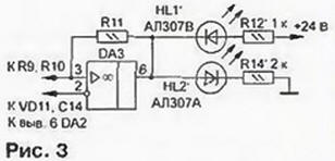
Chip DA5 must be installed on the heat sink. The wires going to the measuring circuit are connected directly to connectors XS1 and XS2. Microcircuits KR140UD708 are interchangeable with KR140UD608 or K140UD6. K140UD7. In place of DA6, OS K140UD6 can be installed. Chip KR142EN5B is replaceable by KR142EN5G. and KR142EN9B - on KR142EN9D or KR142EN9I. It is permissible to replace KR142EN12A with KR142EN12B. but at the same time, the maximum current of the power supply should not exceed 1 A. Transistors VT3 and VT5 KT3102A-KTZ102V. KT3102D or KT315V-KT315E. KT3I5P; VT1. VT2. VT4 and VT6 KT310/A - KT3107D. KT3107I. KT3I07K or KT361V-KT361E. Trinistor VS1 - KU202V-KU202N. Instead of FR207 diodes, you can install domestic KD226 series. Diodes VD13 and VD14 - any KD105 series. KD208 or KD209. In place of the diodes VD11. VD12 and VD15. in addition to that indicated on the diagram, KD521A - KD521V can work. We can replace the HL1 LED with any one with a controlled glow color, rated for a current of 10 ... 20 mA. Transformer - TS-40-2 or another, providing voltage of 12 ... 15 V on windings II and II 'at a current of up to 1.5 A. and on winding III - a voltage of about 10 V. Fixed resistors (except R20) -MLT-0,125 . variables R5 and R8 -SPZ-0a. Resistor R20 is made of a piece of nichrome wire with a diameter of 0.5 mm and a length of 15 cm, wound on an MLT-2 resistor with a resistance of 7,5 kOhm. Oxide capacitors - K50-35. K50-40, the rest - KM. K10-17. Pairs of resistors R18, R22 and R19. It is desirable to select R23 with the least different resistances, and this value itself is not critical - it is quite acceptable to use conventional resistors with a tolerance of 10%. The adjustment of the device consists mainly in the selection of elements that determine the limits of voltage and current changes. By connecting a DC voltmeter to the XS1 and XS2 connectors and setting the variable resistor R5 slider to the upper position according to the diagram, make sure that when the R8 resistor slider is turned, the voltage changes from 0 to 20 V. The upper limit can be set by selecting resistor R7. You should also check the voltage across capacitors C6 and C7. With an output voltage of less than 7 ... 9 V, the capacitors must be charged to a voltage of 15 ... 18 V. and with a higher output voltage - up to 30 ... 35 V. Next, an ammeter is connected to the output of the power source for a maximum current of at least 2 A, and the variable resistor R8 slider is set to the middle position (the resistor R5 slider is in the upper position according to the diagram). When an ammeter is connected, the color of the HL1 LED should immediately change from green to red. If this did not happen and the circuit current does not exceed 1,5 or 1 A (depending on the type of DA5 chip). it means that the built-in protection elements of this microcircuit turned on before the current limiting node on the op-amp DA2. This conflict can be eliminated by reducing the capacitance of the capacitor C15 or increasing the capacitance of the capacitor C16. By selecting resistors R4 and R6, respectively, the upper and lower limits of the change in the limiting current are set at the extreme positions of the engine of the variable resistor R5. It is also necessary to make sure that the current limiting system works with the upper position of the resistor R8 slider according to the scheme. and the voltage on the capacitors C6 and C7 in this case does not exceed 20 V. This completes the adjustment of the device. In the absence of a LED with a controlled glow color, it can be replaced with two different colors, for example, from the AL307 series. while excluding the elements VT2, VD12, R13 and assembling the display unit, as shown in fig. 3.
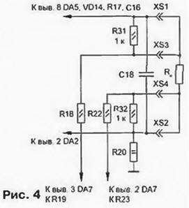
The indication unit can be further simplified by excluding the op-amp DA3, resistors R9 - R11 and turning on the red emission LED in series with the VD11 diode. But in this case, the brightness of the glow will depend on the current overload, and it will be more difficult to notice the moment the device switches to the current stabilization mode. And finally, briefly about how to reduce the influence of the resistance of the conductors connecting the power source to the load. To do this, it is necessary to connect the load Rn (Fig. 4) with four wires. Two of them are power, the other two. connected to connectors XS3 and XS4. connected to the measuring circuit and may have a smaller cross section. Additionally, resistors R31 and R32 should be installed. which will protect the load from overvoltage in the event of a break in the feedback conductors.
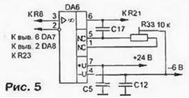
With a four-wire method of switching on the load, it is also advisable to reduce the bias voltage of the op-amp DA6 by introducing a tuned resistor R33 with a resistance of 1 - 10 kOhm, as shown in fig. 5.
By setting the slider of the variable resistor R8 to the lower position according to the diagram, the adjusted resistor R33 sets zero voltage at the output of the power source with an accuracy of fractions of a millivolt. To protect the op-amp DA2 in series with its inverting input, we recommend that you include a resistor with a resistance of about 1 kOhm. Author: A. Shitov, Ivanovo
Machine for thinning flowers in gardens
02.05.2024 Advanced Infrared Microscope
02.05.2024 Air trap for insects
01.05.2024
▪ Robot lizard travels through the sand ▪ The thermal conductivity of copper is improved ▪ The sense of smell makes you fat ▪ Watches on belts instead of gears
▪ section of the site Experiments in chemistry. Article selection ▪ article Folding table. Tips for the home master ▪ article Who are Whigs? Detailed answer ▪ article Cargo trailer for a motorcycle. Personal transport ▪ Article Civil radio communications. Directory
Home page | Library | Articles | Website map | Site Reviews
www.diagram.com.ua |


 Leave your comment on this article: