|
|


 Arabic
 Bengali
 Chinese
 English
 French
 German
 Hebrew
 Hindi
Hindi Italian
 Japanese
 Korean
 Malay
Malay Polish
 Portuguese
 Spanish
 Turkish
 Ukrainian
 Vietnamese
|
ENCYCLOPEDIA OF RADIO ELECTRONICS AND ELECTRICAL ENGINEERING Laboratory DC voltage and current source
Encyclopedia of radio electronics and electrical engineering / Power Supplies that laboratory power source for radio equipment is the result of the practical activities of a small group of guys from the teenage radio engineering club "Radar" (Penza). It is of interest to those who are engaged in the development of equipment based on operational amplifiers and modern microcircuits that require uni- and bipolar supply voltages, regulated over a fairly wide range. A special feature of this laboratory power supply is the protection node. It is known that for some microcircuits designed to be powered by a bipolar voltage source, the situation when one of them is absent is unacceptable. To avoid such situations, the proposed block provides a protection system that blocks the operation of any of the arms of the power supply device in the event of a short circuit in the other arm. After the cause of the short circuit is eliminated, the power supply automatically switches to normal operation. Technical characteristics of the device
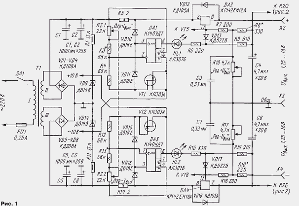
The parameters of the device in the voltage source mode correspond to the reference data for the microcircuit voltage stabilizers used in it [1, 2]. Structurally, it consists of two functionally completed units: a bipolar load power supply and a short circuit protection unit, mounted on separate printed circuit boards. The scheme of the first of these blocks is shown in fig. 1. Windings II and III of the network transformer T1, diode bridges VD1 - VD4 and VD5 - VD8 form a source of bipolar unstabilized voltage + 23 ... 24 V, which supplies all nodes and blocks of the device. The power source of the DA1 microcircuit on its negative terminal is the R11VD14 voltage regulator, and the DA3 microcircuit is the R1VD9 stabilizer.
In terms of operation and circuitry, both arms of the power supply are symmetrical, so let's take a closer look at the operation of only one of them - the positive one. An unstabilized unipolar voltage (not more than +25 V), the ripples of which are smoothed out by capacitors C1 and C2, is fed through the measuring resistor R5, which is included in the measuring bridge, formed by resistors R2.1 - R5 and zener diodes VD10 and VD11, to the input (pin 2) of the microcircuit stabilizer DA2 with output voltage, adjustable variable resistor R10. The measuring bridge is powered by a current source made on a field-effect transistor VT1. While the output current of the stabilizer is less than the set value, the voltage drop across the resistor R5 is small, the voltage at the direct output of DA1 is greater than at the inverse one, and at the output 6 of the op-amp, the voltage is close to +21 V. Diodes HL1 and VD13 are closed and do not affect the operation of the stabilizer DA2. If the output current becomes equal to the threshold value set by the resistor R2.1, the measuring bridge is switched on. OU DA1 goes into linear mode, in which the equality UR2.1 + UR3 = UR5 + Set VD10. In this case, the output voltage of the arm will depend on the voltage at the output of the op-amp, which in turn monitors the voltage drop across the resistor R5, i.e., the load current at which the above equality is satisfied. Therefore, when the ratios R3/R4 = 1 and Ust VD10 = Ust VD11 In = R2.1/R4.Ust VD11/R5. This simplified formula can be used if it becomes necessary to recalculate the parameters of the measuring bridge, taking into account the available element base or other requirements. For more accurate tracking of lower load currents, it is desirable to increase the resistance of the resistor R5. In this case, the upper limit of the load current limit will decrease accordingly. In principle, the negative arm of the power source also works this way. The diagram of the protection unit of the device against a short circuit at its output or in the load is shown in fig. 2. When a bipolar output voltage is applied to its inputs, the transistors VT4 and VT7 open and thereby shunt: the transistor VT4 is the circuit formed by the HL3 LED, the resistor R25 and the emitting diode of the optocoupler U1, and the transistor VT7 is the circuit HL4, R29 and the optocoupler LED U2. Transistors VT3 and VT6 are closed at this time. Such a state of the elements of these circuits of the protection system corresponds to the operation of the device without short circuits in its external circuits.
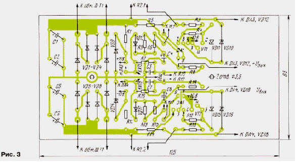
Let's assume that the short circuit occurred in the load connected to the output of the positive arm of the power source. In this case, the transistor VT4 closes. This leads to the opening of the transistor VT6 (through the zener diode VD24 and the resistor R30), which eliminates the mutual blocking of the protection system. Transistor VT7 after blocking the negative shoulder remains an open current flowing into its base through resistor R27 and diode VD23. At the same time, the HL3 LED opens, signaling the occurrence of a short circuit in the + Uout circuit, and the emitter of the optocoupler U1. As a result, the current of the photodiode of this optocoupler increases sharply, the transistor VT8 opens and the collector current blocks the operation of the stabilizer DA4 of the negative arm of the device. This is how a similar part of the protection unit works when the negative arm of the device is shorted in the load. The threshold for operating the protection unit by voltage is determined by the total voltage drop across the diode VD19 (VD22), the emitter junction of the transistor VT4 (VT7), resistor R20 (R26) and in our case is approximately 1 V. You can increase the response voltage by replacing the diodes with the appropriate zener diodes and selecting resistors R20 and R26 for reliable opening of transistors VT4, VT7. Since the voltage at the output of the blocked stabilizers DA2 and DA4 does not exceed 1,3 V, resistors R21, R23, R24, diode VD20, Zener diode VD21 and transistor VT3 of the positive shoulder, as well as similar elements of the negative shoulder, can be excluded, since mutual blocking of the shoulders will not occur . These elements are provided for the case when it is necessary to increase (for the negative arm - to decrease) the voltage of the protection operation threshold. In this case, it is desirable to provide for disconnection from it and the supply voltage of + 10 V. Otherwise, it is impossible to set the output voltage less than the value of the response threshold, since the protection unit will detect a short circuit in the load and block the opposite shoulder. The power supply will work without a protection system. Its printed circuit board is made of one-sided foil fiberglass. The placement of parts is shown in fig. 3. All fixed resistors - MLT, variables R2.1 and R2.2 - double resistor SP3-4aM group A, R10 and R17 - the same group A, but single. Oxide capacitors C1, C2 and C5, C6 - K50-35, C4 and C8 - series K53, C3 and C7 - any ceramic, for example KM-6. Diodes KD208A (VD1-VD8) are interchangeable with similar series KD226, and KD105A (VD12, VD18) - with any of the series KD208, KD209, KD226, diodes VD13 and VD17 - any low-power silicon. The rated stabilization voltage of the zener diodes VD10, VD11 and VD15, VD16 (D818E or KC190 series) can be selected within 9 ... 11 V with minimal thermal drift.
Field-effect transistors VT1 and VT2 (KP303 with the letter index A, B, F or I) are preferably selected according to the initial drain current - within 2 ... 4 mA. Network transformer T1, used in the device from a disassembled foreign-made power supply. Any other will do, including a home-made one that provides an alternating voltage of 17 ... 18 V on each of its secondary windings at a load current of at least 1,4 A. Zener diodes VD11 and VD15 are located on the side of the printed conductors of the board. Stabilizers DA2 and DA4 are mounted on ribbed heat sinks, which are fixed with screws on the printed circuit board from the side of other parts. For better thermal contact, the stabilizers are pre-coated with a layer of heat-conducting paste. The adjustment of the main unit of the device is carried out with the protection unit turned off and consists in a thorough check of the installation and all connections and, if necessary, adjusting the voltages that ensure the operation of the microcircuits and setting up the measuring bridge. Immediately after connecting the device to the network, you should first of all measure the voltage on the filter capacitors C1, C2 and C5, C6, which smooth out the ripples of the bipolar rectifier, and the zener diodes VD9, VD14, which provide power to the op-amp DA1 and DA3. The voltage on the capacitors should not exceed +25 V, and on the zener diodes it should be within +9,5 ... 10,5 V. When the shafts of the resistors R10 and R17 are rotated, the voltages at the corresponding outputs of the power supply arms should change smoothly from up to 1,25 V, and the LEDs HL18 and HL1 do not light up. The maximum values of these voltages are set by a selection of resistors R2 and R8. The functioning of the measuring bridges of the shoulders of the device is controlled by a high-resistance DC voltmeter, connecting it to the input terminals of the op-amp DA1 and DA3. The voltage at the inverted input of each of the op-amps (relative to the common wire) must be more negative than the voltage at the non-inverting input. The difference in the levels of these voltages will change in proportion to the resistances of the resistors R2.1 and R2.2 "Limit Iout". If the voltages are equal, the device must switch from the voltage source mode to the current source mode (or vice versa). The initial value of the load current limit (0,01 A) is achieved by selecting the appropriate resistors (R3 and R13) of the measuring bridges with the shaft of the variable resistor R2 in the position of minimum resistance. The printed circuit board of the protection unit, the placement of parts on it and the connection to the power supply board are shown in fig. 4. All resistors - MLT-0,25. Transistor VT3 - any of the K361 series, and VT6 - any of the KT315 series. The current transfer coefficient of the base of transistors KT3102E (VT4, VT5) and KT3107K (VT7, VT8) must be at least 400.
The mounting boards of the power supply, fastened like a bookcase (Fig. 5), and the network transformer are placed in a case with internal dimensions of 210x90x90 mm from textolite plates 5 mm thick.
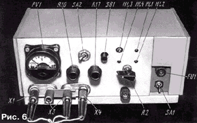
All elements and controls of the unit, as well as socket-clamps for connecting loads and grounding, are located on the front panel of the case (Fig. 6).
There is also a DC voltmeter (PV1 in Fig. 7), which allows you to control the voltage at the output of any of the arms of the power supply.
The power dissipated by the DA2 and DA4 chips must not exceed 10W. This limits the maximum output current of the source to 1,2 A at an output voltage of more than +15 V. With a lower output voltage, the voltage drop across these microcircuits increases, the allowable output current decreases and at an output voltage of 1,25 V is 10 / (24-1,25, 0,44) = 10 A. Each pair of zener diodes VD11, VD15 and VD16, VD10 can be replaced with one zener diode for a voltage of 15 ... a divider of two identical resistors with a resistance of 1 kOhm, connected as zener diodes in the circuit of fig. 3. The use of thermostable zener diodes is not justified, since they are such only at an operating current of 68 mA, and here the current through them is much less. When the unit is operating in the voltage stabilization mode at an output voltage of 1,25 V, the closing bias on the HL1 and HL2 LEDs is about 20 V, which is unacceptable for them. Therefore, any low-power silicon diode should be connected in series with each of them, or simply do not install resistors R9 and R19. Zener diodes VD21 and VD24 for reliable closing of transistors VT3 and VT6 must have a guaranteed higher stabilization voltage than VD9 and VD14, so it is better to use them with indexes G or D. In order for transistors VT5 and VT8 not to be opened by reverse currents of unlit photodiodes U1.2 and U2.2, their base-emitter junctions should be shunted with 510 ... 680 kOhm resistors. Literature
Author: A.Muzykov, Penza
Machine for thinning flowers in gardens
02.05.2024 Advanced Infrared Microscope
02.05.2024 Air trap for insects
01.05.2024
▪ Flash Memory Made from Organic Materials ▪ New Generation of 14nm Intel Processors ▪ Audio-Technica ATH-CKS50TW Wireless Headphones ▪ American attack aircraft powered by alcohol
▪ section of the site for the radio amateur-designer. Article selection ▪ article Computing machine. History of invention and production ▪ article Where is the lake, which hides a whole park under water every year? Detailed answer ▪ article Oyster knot. Tourist tips
Home page | Library | Articles | Website map | Site Reviews
www.diagram.com.ua |


 Leave your comment on this article: