|
|


 Arabic
 Bengali
 Chinese
 English
 French
 German
 Hebrew
 Hindi
Hindi Italian
 Japanese
 Korean
 Malay
Malay Polish
 Portuguese
 Spanish
 Turkish
 Ukrainian
 Vietnamese
|
ENCYCLOPEDIA OF RADIO ELECTRONICS AND ELECTRICAL ENGINEERING Stabilized single-ended voltage converter
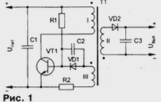
Encyclopedia of radio electronics and electrical engineering / Voltage converters, rectifiers, inverters The article describes the principles of construction and a practical version of a simple pulse stabilized voltage converter that provides operation in a wide range of input voltage changes. Among the various secondary power sources (SEP) with a transformerless input, a single-cycle self-oscillating converter with "reverse" switching on of the rectifier diode is distinguished by its utmost simplicity [1] (Fig. 1).
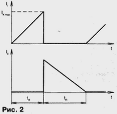
Let us first briefly consider the principle of operation of an unstabilized voltage converter, and then - a method for stabilizing it. Transformer T1 - linear choke; the intervals of energy accumulation in it and the transfer of accumulated energy to the load are separated in time. On fig. 2 shows: II - current of the primary winding of the transformer, III - current of the secondary winding, tn - interval of energy accumulation in the inductor, tp - interval of energy transfer to the load.
When the supply voltage Upit is connected, the base current of the transistor VT1 begins to flow through the resistor R1 (the diode VD1 prevents the passage of current through the base winding circuit, and the capacitor C2 shunting it increases the positive feedback (PIC) at the stage of forming voltage fronts). The transistor opens slightly, the POS circuit closes through the transformer T1, in which the regenerative process of energy accumulation takes place. Transistor VT1 enters saturation. A supply voltage is applied to the primary winding of the transformer, and the current II (collector current Ik of the transistor VT1) increases linearly. The base current IB of a saturated transistor is determined by the voltage on the winding III and the resistance of the resistor R2. At the stage of energy accumulation, the diode VD2 is closed (hence the name of the converter - with the "reverse" switching on of the diode), and power consumption from the transformer occurs only by the input circuit of the transistor through the base winding. When the collector current Ik reaches the value: IK max = h21EIB, (1) where h21E is the static current transfer coefficient of the transistor VT1, the transistor leaves the saturation mode and the reverse regenerative process develops: the transistor closes, the VD2 diode opens and the energy accumulated by the transformer is transferred to the load. After reducing the current of the secondary winding, the stage of energy accumulation begins again. The time interval tp is maximum when the converter is turned on, when the capacitor C3 is discharged, and the voltage at the load is zero. In [1] it is shown that the power supply, assembled according to the circuit in Fig. 1, - functional converter of the supply voltage source Up to the load current source In. It is important to note: since the stages of energy accumulation and its transfer are separated in time, the maximum collector current of the transistor does not depend on the load current, i.e. the converter is completely protected from short circuits at the output. However, when the converter is turned on without load (idle mode), a voltage surge on the transformer winding at the moment the transistor closes can exceed the maximum allowable collector-emitter voltage and disable it. The disadvantage of the simplest converter is the dependence of the collector current IK max, and, consequently, the output voltage on the static current transfer coefficient of the transistor VT1. Therefore, the power supply parameters will vary significantly when using different instances. A converter using a "self-protected" switching transistor (Fig. XNUMX) has a much more stable performance.
The sawtooth voltage from the resistor R3, proportional to the current of the primary winding of the transformer, is applied to the base of the auxiliary transistor VT2. As soon as the voltage across the resistor R3 reaches the opening threshold of the transistor VT2 (about 0,6 V), it will open and limit the base current of the transistor VT1, which will interrupt the process of energy accumulation in the transformer. Maximum current of the primary winding of the transformer II max \u0,6d IK max \u3d 2 / RXNUMX (XNUMX) turns out to be little dependent on the parameters of a particular instance of the transistor. Naturally, the current limiting value calculated by formula (2) must be less than the current determined by formula (1) for the worst value of the static current transfer coefficient. Now consider the issue of the possibility of regulation (stabilization) of the output voltage of the power source. In [1], it is shown that the only parameter of the converter that can be changed to regulate the output voltage is the current IK max, or, what is the same, the energy accumulation time tn in the transformer, and the control (stabilization) unit can only reduce the current compared to value calculated by formula (2). Formulating the principle of operation of the converter stabilization unit, it is possible to determine the following requirements for it:
The schemes of control nodes that implement this algorithm, given in [1], contain a K521SAZ comparator, seven resistors, a transistor, a diode, two zener diodes, and a transformer. Other well-known devices, including television power supplies, are also quite complex. Meanwhile, using a self-protected switching transistor, it is possible to build a much simpler stabilized converter (see the circuit in Fig. 4).
The feedback winding (OS) III and the VD3C4 circuit form a feedback voltage proportional to the output voltage of the converter. The exemplary stabilization voltage of the zener diode VD4 is subtracted from the feedback voltage, and the resulting error signal is fed to the resistor R5. From the engine of the trimmer resistor R5, the sum of two voltages is supplied to the base of the transistor VT2: a constant control voltage (part of the mismatch voltage) and a sawtooth voltage from the resistor R3, proportional to the current of the primary winding of the transformer. Since the opening threshold of the transistor VT2 is constant, an increase in the control voltage (for example, with an increase in the supply voltage Upit and, accordingly, an increase in the output voltage of the converter) leads to a decrease in the current II, at which the transistor VT2 opens, and to a decrease in the output voltage. Thus, the converter becomes stabilized, and its output voltage is regulated within small limits by resistor R5. The stabilization coefficient of the converter depends on the ratio of the change in the output voltage of the converter to the corresponding change in the constant component of the voltage based on the transistor VT2. To increase the stabilization coefficient, it is necessary to increase the feedback voltage (the number of turns of the winding III) and select the VD4 zener diode for the stabilization voltage, which is less than the OS voltage by about 0,5 V. The widespread Zener diodes of the D814 series are practically quite suitable at an OS voltage of about 10 V. It should be noted that in order to achieve better temperature stability of the converter, it is necessary to use a VD4 zener diode with a positive TKN, which compensates for the decrease in the voltage drop at the emitter junction of the VT2 transistor when heated. Therefore, the zener diodes of the D814 series are more suitable than the precision zener diodes D818. The number of output windings of the transformer (similar to winding II) can be increased, i.e., the converter can be made multichannel. Built according to the scheme in Fig. 4 converters provide good stabilization of output voltages when the input voltage changes over a very wide range (150 ... 250 V). However, when operating on a variable load, especially in multichannel converters, the results are somewhat worse, since when the load current changes in one of the windings, the energy is redistributed between all windings. In this case, the change in the feedback voltage reflects the change in the output voltage of the converter with less accuracy. It is possible to improve stabilization when operating on a variable load if the OS voltage is generated directly from the output voltage. The easiest way to do this is to use an additional low-power transformer voltage converter assembled according to any of the known schemes [2]. The use of an additional voltage converter is also justified in the case of a multichannel IVEP. The high-voltage converter provides one of the stabilized voltages (the largest of them - at high voltage, the capacitor filter at the output of the converter is more efficient [1]), and the remaining voltages, including the feedback voltage, are generated by an additional converter. For the manufacture of a transformer, it is best to use an armored ferrite magnetic circuit with a gap in the central rod, which provides linear magnetization. If there is no such magnetic circuit, to create a gap, you can use a gasket 0,1 ... 0,3 mm thick made of textolite or even paper. It is also possible to use ring magnetic circuits. Although it is indicated in the literature that for the diode-reversed converters considered in this article, the output filter can be purely capacitive, the use of LC filters can further reduce the output voltage ripple. For the safe operation of IVEP, a trimming resistor (R5 in Fig. 4) with good motor insulation should be used. The transformer windings, galvanically connected to the mains voltage, must be reliably isolated from the output. The same applies to other radio elements. Like any IVEP with frequency conversion, the described power supply must be equipped with an electromagnetic shield and an input filter. The safety of establishing the converter will be provided by a network transformer with a transformation ratio equal to one. However, it is best to use a series-connected LATR and an isolation transformer. Turning on the converter without load will most likely lead to a breakdown of the powerful switching transistor. Therefore, before proceeding with the adjustment, connect the equivalent load. After turning on, you should first of all check the voltage across the resistor R3 with an oscilloscope - it should increase linearly at stage tn. If the linearity is broken, this means that the magnetic circuit enters saturation and the transformer must be recalculated. Using a high-voltage probe, check the signal at the collector of the switching transistor - the pulse drops should be steep enough, and the voltage across the open transistor should be small. If necessary, adjust the number of turns of the base winding and the resistance of the resistor R2 in the base circuit of the transistor. Next, you can try to change the output voltage of the converter with resistor R5; if necessary, adjust the number of turns of the OS winding and select the VD4 zener diode. Check the operation of the converter when the input voltage and load change. On fig. Figure 5 shows the scheme of the IVEP for the ROM programmer, as an example of using a converter built on the basis of the proposed principle.
Source parameters are given in Table. one. Table 1
When the mains voltage changes from 140 to 240 V, the voltage at the output of the 28 V source is in the range of 27,6 ... 28,2 V; source +5 V - 4,88 ... 5 V. Capacitors C1-C3 and inductor L1 form an input mains filter that reduces the radiation of the high-frequency interference converter. Resistor R1 limits the charging current pulse of capacitor C4 when the converter is turned on. The R3C5 circuit smooths out voltage spikes on the VT1 transistor (a similar circuit is not shown in the previous figures). On transistors VT3, VT4, a conventional converter is assembled, which generates two more from the output voltage +28 V: +5 V and -5 V, as well as the OS voltage. In general, IVEP provides a stabilized voltage of +28 V. The stability of the other two output voltages is ensured by the additional converter being powered from a +28 V source and a fairly constant load of these channels. The IVEP provides protection against exceeding the output voltage of +28 V to 29 V. When exceeded, the VS1 triac opens and closes the +28 V source. The power supply emits a loud squeak. The current through the triac is 0,75 A. Transistor VT1 is installed on a small heat sink made of aluminum plate with dimensions of 40 (30 mm). Instead of the KT828A transistor, other high-voltage devices for a voltage of at least 600 V and a current of more than 1 A can be used, for example, KT826B, KT828B, KT838A. Instead of the KT3102A transistor, you can use any KT3102 series; transistors KT815G can be replaced with KT815V, KT817V, KT817G. Rectifier diodes (except VD1) must be used high-frequency, for example, the KD213 series, etc. It is desirable to use oxide filter capacitors of the K52, IT series. Capacitor C5 must be at least 600 V. Triac TS106-10 (VS1) is used solely because of its small size. Almost any type of trinistor that can withstand a current of about 1 A is suitable, including the KU201 series. However, the trinistor will have to be selected according to the minimum control current. It should be noted that in a particular case (with relatively small current consumption from the source) it would be possible to do without a second converter by building a converter according to the scheme of Fig. 4 with additional windings for +5 V and -5 V channels and linear stabilizers of the KR142 series. The use of an additional converter is caused by the desire to conduct comparative studies of various IVECs and make sure that the proposed option provides better stabilization of the output voltage. The parameters of transformers and chokes are given in Table. 2. Table 2
The magnetic circuit for the T1 transformer is used from the filter inductor of the power supply of the drive on replaceable magnetic disks of the EC series of computers. Types of magnetic circuits of chokes L1-L4 are not critical. The source is established according to the above method, but first the overvoltage protection should be turned off by moving the slider of the resistor R10 to the lower position according to the diagram. After establishing IVEP, it is necessary to set the output voltage to +5 V with resistor R29 and, slowly rotating the slider of resistor R10, reach the opening threshold of the triac VS1. Then turn off the source, turn the slider of the resistor R5 in the direction of decreasing the output voltage, turn on the source and set the output voltage to 5 V with the resistor R28. It should be noted: since the voltages at the outputs +5 V and -5 V depend on the voltage +28 V and are not regulated separately from it, depending on the parameters of the elements used and the current of a particular load, it may be necessary to select the number of turns of the windings of the transformer T2. Literature
Author: Yu.Vlasov, Murom, Vladimir region
Machine for thinning flowers in gardens
02.05.2024 Advanced Infrared Microscope
02.05.2024 Air trap for insects
01.05.2024
▪ Human body for wireless communication ▪ AOC technology will reduce the harm of monitors to vision ▪ New User Identification Methods
▪ section of the site House, household plots, hobbies. Article selection ▪ article With nature alone he breathed life. Popular expression ▪ What were the main features of the Hellenistic era? Detailed answer ▪ article Art director for printing. Job description
Home page | Library | Articles | Website map | Site Reviews
www.diagram.com.ua | ||||||||||||||||||||||||||||||||||||||||||||||||


 Leave your comment on this article: