|
|


 Arabic
 Bengali
 Chinese
 English
 French
 German
 Hebrew
 Hindi
Hindi Italian
 Japanese
 Korean
 Malay
Malay Polish
 Portuguese
 Spanish
 Turkish
 Ukrainian
 Vietnamese
|
ENCYCLOPEDIA OF RADIO ELECTRONICS AND ELECTRICAL ENGINEERING Low power switching power supply, 220/9-10,5 volts 45 milliamps. Encyclopedia of radio electronics and electrical engineering
Encyclopedia of radio electronics and electrical engineering / Power Supplies Scientific and technological progress does not stand still, radio-electronic devices and devices become smaller, losing their volume and mass, and current consumption also decreases. To power some devices, it is enough to have a power source with a power of no more than 400 ... 500 mW, or even less. Power supplies based on low-frequency step-down transformers are gradually being replaced by SMPS. The only thing that remains relevant to this day is the galvanic isolation of the load from the AC mains. The proposed IIP is distinguished by the fact that it is easy to manufacture. At the same time, it provides galvanic isolation of the load from the AC mains and withstands the short circuit of the output. The disadvantages include low stabilization of the output voltage, but if necessary, this disadvantage can be eliminated by using a low-power integrated voltage regulator of the 78Lxx series or similar. Technical specifications
The scheme of the device is shown in fig. 1. Its basis is the IR2153D chip, which is a driver with a built-in oscillator. This microcircuit is designed to control two series-connected switching field-effect transistors and build powerful pulse voltage converters. The output stages of the driver are connected so that they are powered in parallel, as a result of which they work as two half-bridge switches in antiphase. When connecting a pulse transformer to the outputs of these stages - NO and LO (terminals 7 and 5) - a bridge circuit of the voltage converter is obtained.
The driver is powered from the AC mains through a quenching capacitor C1, a current-limiting resistor R2 and a rectifier based on diodes VD1-VD4. The ripple of the rectified voltage is smoothed out by the capacitor C2. Resistor R1 ensures the discharge of the capacitor C1 after the power supply is disconnected from the network. The supply voltage is stabilized by a built-in 15,6 V zener diode. The conversion frequency is set by the R3C3 circuit, it can be determined by the formula: F \u1d 1,4 / (3C3 (R75 + XNUMX Ohm)) With the ratings indicated on the diagram, the conversion frequency is about 70 kHz. The output stages of the DA1 driver provide an output pulse current of up to 200 mA. which makes it possible to connect the primary winding of the transformer T1 directly to the outputs of the microcircuit. The alternating voltage of the secondary winding is supplied to the rectifier with voltage doubling, assembled on diodes VD5, VD6 and capacitors C4, C5. The presence of the output voltage is signaled by the LED HL1. Resistors MLT, C2-23, capacitor C1 type K73-17 or imported are used in the IIP, it must be designed to operate at an alternating voltage of at least 400 V, capacitor C3 - K10-17 or SMD, the rest are oxide capacitors domestic or imported. Diodes 1N4007 can be replaced with 1N4005, 1N4006 or a low-power diode bridge designed to operate on a 220 V network, for example, KTS407A. Schottky diodes 1N5819 are interchangeable with 1N5817, 1N5818 or diodes of the KD510, KD521, KD522 series, but in the latter case, the output voltage will decrease by about 1 V. The HL1 LED can be of any glow color. The transformer is wound on a magnetic circuit of size R10x6 x4 (EPCOS B64290L0038-N87) made of ferrite with a magnetic permeability of 2200. A PELSHO wire with a diameter of 0,12 mm is used. The primary winding is wound turn to turn in one row - this is approximately 85 turns (a deviation of ± 10 turns is allowed). To increase the reliability of the insulation, the primary winding is covered with 2 ... 3 layers of varnish; for this purpose, an aerosol automotive acrylic varnish is used, which has an increased resistance to atmospheric and mechanical influences. Then the secondary winding is wound - 30 turns also turn to turn in one row. The printed circuit board for the device was not developed. All parts are placed on a breadboard printed circuit board using wired wiring (Fig. 2). The board is placed in a plastic case measuring 60-35-25 mm. It is necessary to make holes in the case for the LED, network and output cables.
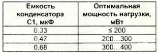
The output power of the power supply depends on the capacitance of the quenching capacitor C1. The table shows its capacity for various values of output power.
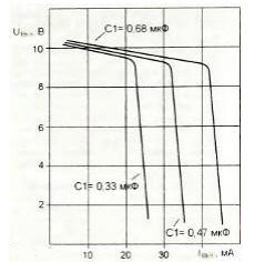
The load characteristics of the source are shown in fig. 3.
If the power consumed by the load is less than optimal, the excess energy will be used to heat the microcircuit. After assembly, the device does not need to be configured and can immediately be used to power the corresponding load. Author: Deparma A.
Machine for thinning flowers in gardens
02.05.2024 Advanced Infrared Microscope
02.05.2024 Air trap for insects
01.05.2024
▪ A class of materials with variable mechanical properties has been created ▪ Ion-optical quantum microscope sees individual atoms ▪ British nutrition is deteriorating ▪ The universe is threatened by dark energy
▪ section of the site Reference materials. Article selection ▪ article Budgetary system of the Russian Federation. Lecture notes ▪ article What is a fruit fly? Detailed answer ▪ article Banksia is bright red. Legends, cultivation, methods of application ▪ article Electrical stimulator for fish. Encyclopedia of radio electronics and electrical engineering
Home page | Library | Articles | Website map | Site Reviews
www.diagram.com.ua |


 Leave your comment on this article: