|
|


 Arabic
 Bengali
 Chinese
 English
 French
 German
 Hebrew
 Hindi
Hindi Italian
 Japanese
 Korean
 Malay
Malay Polish
 Portuguese
 Spanish
 Turkish
 Ukrainian
 Vietnamese
|
ENCYCLOPEDIA OF RADIO ELECTRONICS AND ELECTRICAL ENGINEERING Laboratory power supply with diagnostics. Encyclopedia of radio electronics and electrical engineering
Encyclopedia of radio electronics and electrical engineering / Power Supplies Having chosen the scheme of an electronic device that has attracted, each radio amateur first tries it in operation. Then you can make the device you like or (having experience) make additional improvements to it. In both cases, a power source is needed. You can buy it or win the lottery, but it's best to make it yourself. At the same time, the radio amateur's laboratory will be replenished with a device not only with basic, but also with additional useful functions. Using the example of a power source, let's try to trace the entire process of designing and manufacturing an amateur radio electronic device. The output voltage is constant. But with the magnitude of it must be dealt with. Basically, all the above circuits use a voltage of 12 V. However, the KR1156EU5 microcircuit, like other microcircuits, can operate at other voltages. Therefore, a wider output voltage range should be provided in the power supply for experimental work. And it would be better if it could be regulated. Next, you need to solve the question, but within what limits to change the output voltage? Knowledge of the KR1156EU5 chip, which this book tells about, will help here. The minimum operating voltage for it is 3 V. The nominal voltage for most devices is 12 V. Therefore, the power supply must provide an output voltage of 3 to 12 V? Let's not rush to conclusions, but take a broader look. A margin is needed, especially since the microcircuit allows you to work at a higher supply voltage (after all, it can be up to 40 V). Also, if you experiment with the KR1436AP1 microcircuit, you may need not only a voltage of 12 V, but also up to 27 V. But we will not aim at such a large value, but we will limit ourselves to the output voltage range of our source from 3 to 15 V. This will provide power not only to analog microcircuits, such as operational and low-frequency amplifiers, but also digital microcircuits, both TTL and CMOS . Now we need to decide on the load current. Most of the considered devices consume a small current (approximately 10 ... 50 mA). They can be powered from ready-made low-power adapters. However, we will not be limited to such a current, but will make the device "for growth", more powerful. Having decided on the main parameters of the output voltage of the power supply, let's take a look at its structure, i.e., consider what main and auxiliary nodes it should consist of. Due to the fact that the source of electricity in our apartments is an alternating current network, a source of increased danger, an isolation transformer is needed. It is also called power. It is necessary in order to transfer (transform) the energy of the network. This is its main function. In addition, the transformer converts the high voltage in the network (220 V) into a low secondary voltage (12 ... 15 V). But to power electronic devices, a constant voltage is required and an appropriate converter is needed. Therefore, a secondary AC to DC rectifier is required. The ripple voltage after the rectifier is smoothed out by the filter. The simplest filter is a conventional large capacitor. One part of the power supply has been identified - this is a transformer, a rectifier and a filter. Due to the fact that the mains voltage is unstable, there are sharp jumps and slow drops, and this is unacceptable for electronic circuits, you will need a node that provides a stable supply voltage. It's called a stabilizer. As you know, they are impulse and linear. Given the scope - experimental work - the power supply should be able to adjust the output voltage. As is to be expected, errors can occur during prototyping and testing, so protective measures must be taken to protect the power supply and load from hazardous operating conditions. One such measure, which is most commonly used in electronics, is current limiting. In this case, it is necessary to provide for limiting the load current so that if it is exceeded or even a short circuit (short circuit) does not fail (or even burn out) the power source. It is also desirable to be able to set a specific current limit. Prolonged overloading of the power supply is dangerous even with a protection circuit. Therefore, it is necessary to have an additional unit for prompt indication (by sound or light signal) of a dangerous mode. So we have decided on the structure of a network stabilized single-channel power supply with protection. Let's list its nodes again:
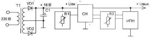
The next task is to determine the element base of our device. On what elements and in what modes of their operation will the achievement of the main goal of our project be ensured - providing a supply voltage for amateur radio work. A microcircuit of the type KR1156EU5 known to us in the mode of a pulsed step-down stabilizer may well provide the required output parameters (3 ... 12 V, 0,1 ... 0,5 A). A few watts of power necessary to power the load will be "pulled" by a unified transformer of the TP112 type. It is rated at 7,2 W and is designed for PCB. These transformers are available for a range of output voltages and it is quite possible to choose the right one for our case. The output voltage can be adjusted continuously or stepwise. For convenience, we choose a stepwise way to set the output voltage. A light press on the button - and you always know what voltage is supplied to the load. And as a switch (adjustment body), a sectioned push-button switch of the P2K type is applicable. Similarly, we construct a load current limiting node. We also apply stepwise switching using P2K. The experience gained in the use of the KR1156EU5 microcircuit tells us that the indicator for lowering the output voltage beyond the permissible limits can also be designed on its basis. Having decided on the main nodes and the element base of the designed power source, you can draw up its block diagram. The scheme shown in fig. 5.14 is quite consistent with our project.
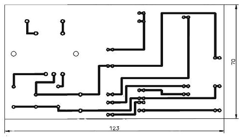
The main ones in this circuit are a network (isolating) transformer with a full-wave rectifier and a filter and a voltage stabilizer (SN). At the output of the stabilizer, an undervoltage indicator (PV) is turned on. Two control nodes are also provided here: limiting current (R1) and output voltage (R3). The developed block diagram of the power supply with the necessary functions for the radio amateur laboratory also sets the features of the design. After all, the design of the power source should provide convenience when working with it. It is also necessary to ensure quick repair in case of failure. Indeed, the power supply requires uninterrupted operation and a minimum recovery time after a loss of performance. In this case, the modular design of the device is quite acceptable. Its peculiarity lies in the fact that a transformer and a filter capacitor (the largest elements) and other nodes (SN, PPN, etc.) are installed on a common board. Each of these nodes is located on a separate printed circuit board. If necessary, each node can be disconnected from the common board and repaired. To obtain the minimum volume of the entire structure, the printed circuit boards of the nodes should be placed vertically on the common board. They can even be installed in special slots. This decision is also pushed by the fact that the switching of modes is carried out by switches L2K. Being installed on a printed circuit board, they seem to "lie" on it, occupying a large area. Therefore, placing the board with P2K vertically and with the buttons up will lead to a decrease in the area occupied on the overall board. Thus, the volume of the device will be filled rationally. The total fee will have a minimum size. And the size of the boards of individual nodes will be determined on the one hand by the total board (width), and on the other hand, by the height of the P2K switches and the transformer (height). In accordance with the block diagram of our device, on the main board with a transformer, a rectifier and a filter capacitor, the following are installed:
To expand the functionality of the power supply, you can additionally provide for the installation of a board with a linear voltage regulator chip. This will allow you to have a second voltage with independent adjustment. In addition, at this output, the voltage will have a lower level of ripple, which is necessary when working with sound amplifying devices. In view of the foregoing, the total fee will have the form shown in Fig. 5.15. The massive transformer is attached to the board with two self-tapping screws, for which mounting holes are provided. In addition, the leads of the transformer windings, soldered to the board, also create an additional fastening.
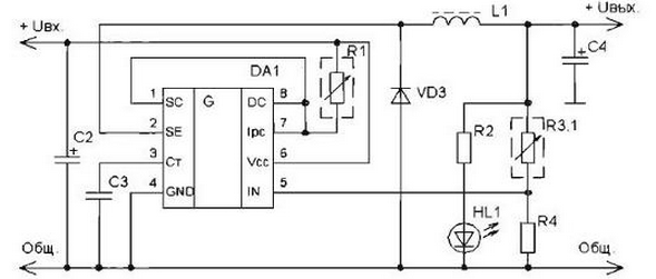
If possible, the connection of the network wire can be done using special contacts. How the network part of the power supply is built is clear from the diagram in Fig. 5.14. The scheme of the main node - voltage stabilizer (SN) - is shown in fig. 5.16.
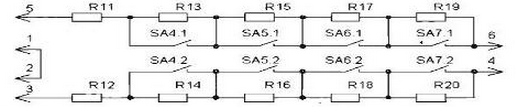
CH is made according to the scheme of a pulsed step-down stabilizer based on the KR1156EU5 microcircuit. It is conditionally shown here that it is possible to change the value of the limiting current (R1) and adjust the output voltage (R3). The limiting current or the maximum load current is set using the regulating element (R1). A detailed diagram of the switches and a set of resistors is shown in fig. 5.17.
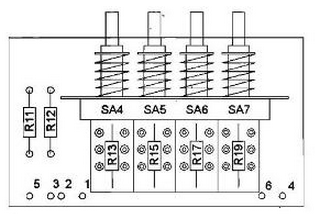
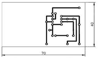
The electrical circuit consists of switches SA1-SA3<П2К) and resistors R5-R10. The peculiarity of such a circuit is that all resistors of the same rating are used (R \u1d XNUMX Ohm). The maximum load current (approximately 600 mA) will be with all switches closed when the resistance R1 is 0,5 ohms. Accordingly, the current will be equal to 300 mA (with SA1 open), 150 mA (with SA1 and SA2 open), 100 mA (with SA1, SA2 and SA3 open). Switches. P2K should have an independent fixation and then you can press more than one button. Other combinations of pressed buttons are also possible, which will correspond to other limiting currents. It is up to the reader to determine these additional limiting current values. One feature should be noted. The diagram has a jumper 1-3. It is designed to exclude a dangerous mode during repair work and with an uninstalled current control board and accidental supply voltage. Since the jumper is connected in series to the input circuit of the stabilizer, if it is not present, the switching buck regulator board will be de-energized. The output voltage of the switching buck regulator is adjusted by a resistor in the upper arm of the feedback divider (R3.1). It is also made on P2K switches and resistors. The values of these resistors are calculated in such a way that the output voltage can change in steps of 1 V. You can get by with fewer parts by choosing the ratio of resistor values (R13: R14: R15: R16) according to the binary law: 1-2-A-8. Thus, with the help of a partitioned resistor, the circuit of which is shown in Fig. 5.18, you can set the value of the upper arm of the divider in both CH and PPN. In this case, the output voltage can have a value from 3 to 18 V, since. resistance varies from 1,8 kΩ to 16,8 kΩ (1,8 kΩ + 15 kΩ).
We only add that the diagram shows not only a divider for SN, but also a divider for PPN. We will review his work later. Jumper 1-2 is also designed to prevent dangerous operation in the absence of a board with dividers and accidental voltage supply. The accepted ratio of resistor values predetermines the corresponding work with switches. For example, you need to set the output voltage to 5 V. With all switches closed (SA4, SA5, SA6 and SA7), the output should be 3 V. Therefore, you need to add 5 - 3 = 2 V, i.e. SA5 must be open and R15 = 2 kΩ included in the circuit. The other necessary voltage at the output is set similarly. Due to the fact that the switches are paired, there are changes in the other divider. It is designed for PSI and is made in the same way with the same ratios of resistors. Let's consider the scheme of the output voltage decrease indicator, which is shown in fig. 5.19.
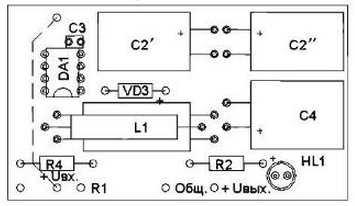
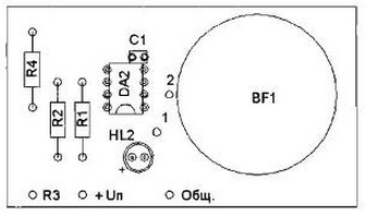
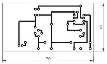
The main part of the undervoltage indicator is the KR1156EU5 microcircuit. It works in pulse generator mode. Let us briefly consider the functioning of this auxiliary, diagnostic, node. The comparator of the microcircuit compares the unstable voltage of the power supply (at input 5) with the stable voltage of the reference voltage source. Depending on the ratio of these voltages, the operation of other components of the microcircuit is controlled. In the event that the power supply voltage is normal (the potential of pin 5 exceeds 1,25 V), the comparator turns the output transistors into a non-conductive state. The red LED (HL2) is off. When the voltage drops, the comparator switches and the internal oscillator starts to work. The output transistors alternately go from open to closed, and the red LED flashes periodically. The current through it sets the resistor R21. At the same time, an audible signal appears, because. piezo BF1 starts to click when switching transistors. Thus, an electronic device - a voltage drop indicator - constantly monitors the output voltage of the power source and attracts attention with light and sound signals when it decreases in the event of an overload. And this is possible when the set load current is exceeded and the MV protection circuit is triggered. In addition, the indicator will also work in the absence of output voltage at the CH output. Thus, if during repair work any board with partitioned resistors is accidentally not installed (and the CH board is de-energized), then the sound signal will draw your attention to this. The intended functions are implemented and the layout of the laboratory power supply is thought out. Now we need to design the nodes that are located on separate printed circuit boards and mounted on the main board with a transformer. The switching buck regulator board (Figure 5.20) is located closest to the rectifier. This reduces the length of the conductors through which the load current flows. To reduce ripples and increase the stability of the stabilizer, in addition to the main filter capacitor (C1), this board also has a capacitor C2 (composed of two - C2 'and C2 "). Thus, the overall dimensions of the board are reduced. With one capacitor, the height of the board was would be more.
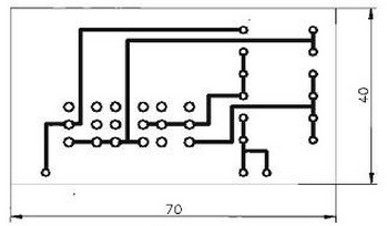
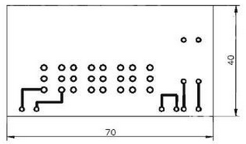
Another feature of the board design is that the storage filter choke is made on cylindrical small-sized unified chokes of the DM (DPM) type. To obtain the required inductance, up to 3 DM type chokes are connected in series. The output voltage indicator on the HL1 LED can be installed on the front panel of the power supply housing and connected to the switching regulator board by wires. The load current limit is set using a partitioned resistor located along with switches on the board shown in fig. 5.21. The MV output voltage and the pick-up voltage of the PSU are set using a sectioned switchable resistor, the details of which are located on the board shown in fig. 5.22. Switches. P2K are installed horizontally in the holes on the board and they are fixed not with screws, but with the help of soldering. And the resistors of the upper arm of the divider are mounted in a hinged way on the P2K terminals. In this case, the resistors of each divider are located on different sides and are connected to the board with wires. And, finally, on the common board there is also an indicator for lowering the voltage at the output of the CH, the location of the elements of which is shown in Fig. 5.23. The BF1 piezo emitter is soldered directly to the board. The HL2 LED, which indicates a dangerous mode of operation of the power supply, can be installed on the front side of the case and connected to the board with wires.
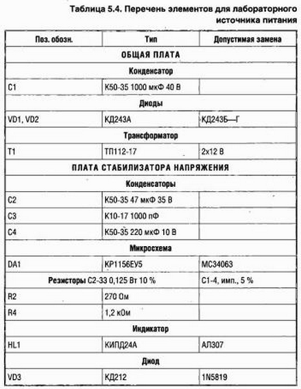
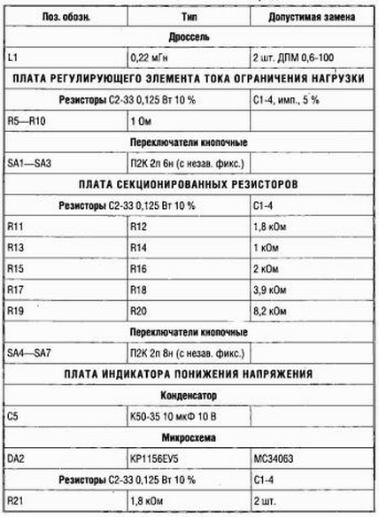
There are two options for fixing printed circuit boards on a common board. First, you can install connectors on a common board that are specially designed for direct connection to a printed circuit board (SNP14). Secondly (and this method is simpler), it is possible to fix individual nodes vertically using brackets made of uninsulated tinned copper wire with a thickness of 0,8-1,0 mm. It is soldered to the board and bent on both sides. And then all the brackets are installed in the holes of the common board and also soldered. A significant drawback of the second method is obvious: the permanent connection does not allow you to quickly disconnect the faulty unit for repair operations. Despite its complexity, the first method (with connectors) is more suitable for a sophisticated version of a laboratory power supply. If you want to add a stabilized voltage output with low ripple, then this will require the installation of another board with a linear regulator. It could be a positive voltage regulator. However, quite often a negative voltage is also required, for example, to power op-amp chips. Therefore, you will also need a place to install a board with a stabilizer chip for a negative voltage. For convenience, you can also apply the installation of fixed output voltages using partitioned resistors. When a power source is conceived not with a limited set of functions, but with their subsequent increase through gradual modernization, then the design should also provide for the appropriate capabilities. Foresight in this matter and an increase in the size of the main board for installing additional node boards will make it relatively easy to modify the power supply to increase the functions performed if the need arises. The manufacture of our version of the power source must begin with the selection of the required components. Their list is given in Table. 5.4. All the necessary radio components are collected here, but with a division into boards of individual nodes.
The next stage of manufacturing is the verification of all radio elements. If this condition is met, there will be confidence that after assembly the device will work, and you will not have to waste time troubleshooting due to low-quality elements and dismantle them. Of course, printed circuit boards are also needed. They are made of foil-coated one-sided textolite 1,5 mm thick according to the sketches shown in fig. 5.24-5.28. The use of printed circuit boards facilitates the installation of radio elements, but their manufacture is associated with certain skills and the use of chemicals. You can go on another, cheaper and easier way. Having carefully looked at the drawings of conductors on the sketches of printed circuit boards, you can see that the installation is simple and can be carried out in a hinged way. Moreover, this is facilitated, for example, by the presence of hard leads on the transformer, P2K switches and other elements. They can be successfully used both for direct connection of elements to each other, and for fixing mounting conductors. After mounting the elements on the boards, it is necessary to carefully check the correct installation (especially polar elements) and the quality of the connections. After making sure that there are no errors, you can proceed to the next step in the manufacture of the power supply. It consists in an autonomous check of each board. You should start with a general fee. Having applied mains voltage to the primary winding of the transformer, it is necessary to measure the DC voltage across the filter capacitor.
After making sure that this part of the device is functioning correctly, it is necessary to carry out another test under load. To do this, a 27 Ohm (2 W) resistor is connected to the rectifier output to provide a load current of 0,4 ... 0,6 A and the output voltage is checked again. Its value should be approximately 12 V. After confirming that the rectifier board is working properly, it can be used to check the operation of the MV board. However, before applying voltage to the CH, it is necessary to put a jumper between the contacts of the board connecting the pins of the microcircuit 6 and 7, i.e., exclude the load current limiting resistor (R1). It is also necessary to install a temporary output voltage divider (for feedback). A resistor of 6,8 kΩ should be in place of the resistor R3.1 between pin 5 of the microcircuit and the CH output After all these preparatory operations, you can apply the input voltage and check the operation of the CH at RH = 200 Ohm, i.e. at a small load current (ln - 40 mA). The power of this resistor must be at least 0,5 watts. In this mode, we measure the output voltage of the CH, its value should be approximately in V. The next step is to check the stability of the output voltage when the load changes. To do this, we connect in parallel with the load resistor the same one (200 Ohms), i.e. we get RH = 100 Ohms. In this case, the load current will double and will be approximately 80 mA. Having measured the output voltage again, you need to make sure that it changes in accordance with the parameters of the microcircuit and that the entire assembly is working properly. Now we need to check the board of partitioned resistors. This can be done with a multimeter (digital tester). After making sure that when a certain button is pressed, the total value of the resistor measured by the device corresponds to the design value, this board can be set to general. Next, they similarly check the board with resistors of the load limiting current control element (R5-R10) and also install it on a common board. When all three boards are installed on a common board: a voltage stabilizer, sectioned dividers and a load limiting current control element, then you can proceed to a comprehensive check of the functioning of a fully assembled ISN without a network part. This can be done with an optional regulated power supply. To simplify the test, the network part of our power supply can be used as this, but it must be taken into account that some parameters (for example, voltage stability) cannot be checked. The sequence for checking the assembled power supply is as follows:
Now it remains to strengthen the common board assembly inside the case and make connections to the output terminals. Having finally made sure that all parameters are normal, you can start working with the power source. Author: Koltsov I.L.
Machine for thinning flowers in gardens
02.05.2024 Advanced Infrared Microscope
02.05.2024 Air trap for insects
01.05.2024
▪ New product labeling technology ▪ Wheelchair control with the mind ▪ Powder that purifies water from E. coli ▪ Budget 8" tablet Archos 80 Xenon on Android 4.1
▪ section of the Radio Control website. Article selection ▪ article No need to fight for cleanliness, you need to sweep! Popular expression ▪ article How long can a person born with a mirror image of internal organs live? Detailed answer ▪ Sapindus article. Legends, cultivation, methods of application ▪ article Car subwoofer. Part 2. Encyclopedia of radio electronics and electrical engineering
Home page | Library | Articles | Website map | Site Reviews
www.diagram.com.ua |


 Leave your comment on this article: