|
|


 Arabic
 Bengali
 Chinese
 English
 French
 German
 Hebrew
 Hindi
Hindi Italian
 Japanese
 Korean
 Malay
Malay Polish
 Portuguese
 Spanish
 Turkish
 Ukrainian
 Vietnamese
|
ENCYCLOPEDIA OF RADIO ELECTRONICS AND ELECTRICAL ENGINEERING Economic stabilizer with protection system. Encyclopedia of radio electronics and electrical engineering
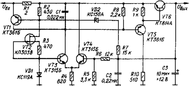
Encyclopedia of radio electronics and electrical engineering / Surge Protectors Voltage stabilizers with a falling characteristic of the protection system have the ability to automatically return to the voltage stabilization mode after the overload cause has been eliminated; relatively little power is dissipated on the regulating element in the load closing mode. Such a stabilizer usually contains a reference voltage source, a differential amplifier, a protection system, and a control element on a composite transistor. The protection system includes a load current limiter and a circuit with a zener diode connected in parallel to the regulating element. This circuit forms the falling section of the load characteristic. The load current limiter is built on a current-measuring resistor connected between the base and the emitter of the transistor, shunting the emitter junctions of the regulating element. The disadvantage of these stabilizers is a significant difference between the input and output voltages, which is necessary for the normal operation of the device. It consists of a voltage drop across the current source in the collector circuit of the differential amplifier and the emitter junctions of the compound transistor of the regulating element and is approximately 3 V. Such a large value does not allow achieving a high efficiency of the device, especially at low output voltage. For example, a 5-volt regulator made according to a similar scheme will have an efficiency of about 60%. The voltage drop across the stabilizer can be reduced to 1 ... 1,5 V if a germanium transistor is used in the current source in the collector circuit of the differential amplifier, and a composite transistor with additional symmetry is used in the control element. Even more increase the efficiency of the stabilizer allows its construction according to the scheme "with low loss voltage". The composite control transistor must be connected here according to the circuit with a common emitter with respect to the load, therefore, the inverting output of the differential amplifier is used to control the control element. In this case, there is no need for a current source, since the collector current from this output of the differential amplifier directly serves as the base current of the composite transistor of the regulating element. The minimum difference between the input and output voltages, sufficient for the normal operation of the stabilizer, is equal to the voltage drop across the current-measuring resistor plus the saturation voltage of the output transistor and does not exceed 1 V. There is only one way to further reduce the loss voltage on the stabilizer - by reducing the voltage drop across the current-measuring resistor. This possibility is implemented in the stabilizer, the scheme of which is shown in Fig.1.
Resistor R2 of the protection device is included in the current source circuit, made on a field-effect transistor VT2. The maximum output current Imax of the stabilizer is determined by the expression Imax ~ (0,6-UR2) / R1, where UR2 is the voltage drop across the resistor R2. By selecting resistor R3, the current through resistor R2 is set to 1 mA. Thus, the maximum voltage drop across the resistor R1 is approximately 0,2 V. The main technical characteristics of the stabilizer:
Temperature coefficient of the output voltage, %/° С ~ -0,35 The type of load characteristics of the stabilizer at different values of the input voltage is shown in Fig. 2.
The limits for changing the input voltage can be expanded upwards by using a VD2 zener diode with a higher stabilization voltage. In this case, however, the load characteristic will change somewhat. The stabilizer has a certain versatility. The output voltage can be changed by selecting the resistor R6 in the range from Uo6p + (2 ... 3) V to the maximum allowable voltage Uke of the transistors used (Uobr - reference voltage). These 2 ... 3 V are necessary for the operation of the current source collected on the transistor VT2. The required form of the load characteristic is achieved by a selection of elements VD2 and R7. The maximum load current is set by selecting the resistor R1. Without any changes, the stabilizer can operate at a load current of up to 1 A. With an even higher current, the composite regulating transistor should no longer be double, but triple - an even more powerful transistor will have to be added. The stabilizer can also use other low-power silicon transistors of the appropriate structure, suitable for voltage. The KT814A transistor can also be replaced by another, pnn structure, designed for the corresponding power dissipation. Use transistors with low saturation voltage. The described stabilizer can be recommended for use in devices where the requirements for the stability of the output voltage are moderate, and the main factors are high efficiency and the presence of protection against overloads and short circuits in the load with automatic return to operating mode after the overload is eliminated.
Artificial leather for touch emulation
15.04.2024 Petgugu Global cat litter
15.04.2024 The attractiveness of caring men
14.04.2024
▪ Dust and water resistant smartphone LG Optimus GJ ▪ Adata Industrial Grade Solid State Drives ISSS332 ▪ The Ultimate Weapon Against Insects
▪ section of the website Basics of First Medical Aid (BFA). Selection of articles ▪ article Augean stables. Popular expression ▪ article Which plant can copy the leaves of many other plants on the same shoot? Detailed answer ▪ article Bicycle computer. Travel Tips ▪ article Homemade wind generator. Encyclopedia of radio electronics and electrical engineering
Home page | Library | Articles | Website map | Site Reviews
www.diagram.com.ua |


 Leave your comment on this article: