|
|


 Arabic
 Bengali
 Chinese
 English
 French
 German
 Hebrew
 Hindi
Hindi Italian
 Japanese
 Korean
 Malay
Malay Polish
 Portuguese
 Spanish
 Turkish
 Ukrainian
 Vietnamese
|
ENCYCLOPEDIA OF RADIO ELECTRONICS AND ELECTRICAL ENGINEERING Power supplies: micro power, medium power, high power. Encyclopedia of radio electronics and electrical engineering
Encyclopedia of radio electronics and electrical engineering / Power Supplies The first problem that both beginners and experienced radio amateurs face when designing any device is the problem of power supply. This chapter will cover a variety of mains power supplies (micro power, medium power, high power). When choosing and developing a power source (hereinafter referred to as PI), it is necessary to take into account a number of factors determined by operating conditions, load properties, safety requirements, etc. First of all, of course, you should pay attention to the compliance of the electrical parameters of the power supply with the requirements of the powered device, namely:
The characteristics of the IP that affect its performance are also important:
Being an integral part of radio-electronic equipment, secondary power supplies must strictly comply with certain requirements, which are determined both by the requirements for the equipment itself as a whole, and by the conditions for power sources and their operation as part of this equipment. Any of the IP parameters that go beyond the limits of acceptable requirements introduces dissonance into the operation of the device. Therefore, before starting the assembly of the IP to the proposed design, carefully analyze all the available options and select the IP that will best meet all the requirements and your capabilities. There are four main types of mains power supplies:
converter 20-400kHz. Linear power supplies are characterized by extreme simplicity and reliability, the absence of high-frequency interference. The high degree of availability of components and ease of manufacture make them the most attractive for repetition by novice radio designers. In addition, in some cases, a purely economic calculation is also important - the use of linear IPs is clearly justified in devices that consume up to 500 mA, which require fairly small-sized IPs. Such devices include:
It should be noted that some designs that do not require galvanic isolation from the industrial network can be powered through a quenching capacitor or resistor, while the current consumption can reach hundreds of mA. The efficiency and rationality of the use of linear power supplies is significantly reduced at consumption currents of more than 1 A. The reasons for this are the following phenomena:
Secondary pulse voltage converters are quite simple in manufacture and operation, they are distinguished by ease of manufacture and low cost of components. It is economically and technologically justified to design a power supply according to the scheme of a secondary pulse converter for devices with a current consumption of 1-5 A, for uninterrupted power supply for video surveillance and security systems, for low-frequency amplifiers, radio stations, chargers. The best distinguishing feature of secondary converters over linear ones is the weight and size characteristics of the rectifier, filter, converter, stabilizer. However, they are distinguished by a high level of interference, therefore, when designing, it is necessary to pay attention to shielding and suppression of high-frequency components in the power bus. Recently, pulsed IP, built on the basis of a high-frequency converter with a transformerless input, have become quite widespread. These devices, powered by an industrial network ~ 110V / 220V, do not contain bulky low-frequency power transformers, and the voltage is converted by a high-frequency converter at frequencies of 20-400 kHz. Such power supplies have an order of magnitude better mass-dimensional parameters compared to linear ones, and their efficiency can reach 90% or more. IP with a pulsed high-frequency converter significantly improve many characteristics of devices powered by these sources, and can be used in almost any amateur radio design. However, they are distinguished by a rather high level of complexity, a high level of noise in the power bus, low reliability, high cost, and unavailability of some components. Thus, it is necessary to have very good reasons for using pulsed IP based on a high-frequency converter in amateur equipment (in industrial devices, this is in most cases justified). Such reasons can be: the probability of fluctuations in the input voltage within ~ 100-300 V; the ability to create an IP with a power from tens of watts to hundreds of kilowatts for any output voltage; the emergence of affordable high-tech solutions based on ICs and other modern components. 1. Power supply with galvanic isolation from the network on optocouplers Micropower IPs with galvanic isolation from the ~220 V mains can be made using optocouplers by connecting them in series to increase the output voltage (Fig. 3.2-1.). Energy transfer is carried out by means of a unidirectional light flux inside the optocoupler (the optocoupler contains light emitting and absorbing elements), so there is no galvanic connection with the network. On one optocoupler, 0,5-0,7 V is allocated for AOD101. AOD302 and 4 V - for AOT102, AOT110 (inflow 0,2 mA). To provide the required values of voltage and current, optocouplers are connected in series or in parallel. As a buffer accumulating element, you can use an ionistor, a battery or a capacitance of 100-1000 microfarads. The LEDs are powered through a capacitance of no more than 0.2 uF to avoid destruction. It must be remembered that the efficiency of optocouplers decreases over time (approximately 25% over 15000 hours of operation).
2. Micro power stabilizer with low consumption Some ham designs require micropower regulators that consume microamps in stabilization mode. On fig. 3.2-4 shows a schematic diagram of such a stabilizer with an internal current consumption of 10 μA and a stabilization current of 100 mA.
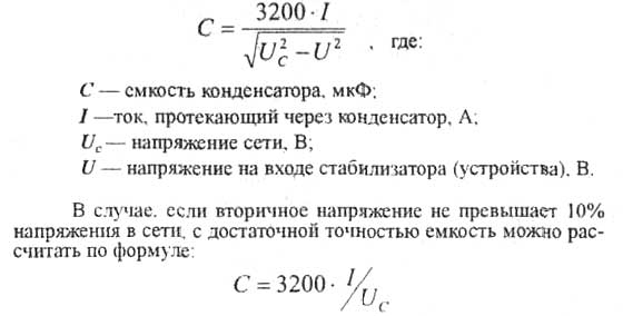
For the elements indicated in the diagram, the stabilization voltage is Uout \u3.4d 1 V, to change it, instead of the HL522 LED, you can turn on KD0.7 diodes in series (on each voltage drop is 1 V: on transistors VT2, VT0,3 - 30 V). The input voltage of this stabilizer (Uin) is not more than XNUMX V. Transistors with a maximum gain must be used. 3. Power supplies with coupling capacitors In micropower power supplies with galvanic coupling to an industrial network, so-called. coupling capacitors, which are nothing more than shunt resistors connected in series in the power circuit. It is known that a capacitor installed in an alternating current circuit has a resistance that depends on frequency and is called reactive. The capacitance of the isolation capacitor (assuming application in an industrial network ~ 220 V, 50 Hz) can be calculated using the following formula:
For example: a charger for 12V nickel-cadmium batteries with a capacity of 1 Ah can be powered from the mains through a separating capacitor. For nickel-cadmium batteries, the charging current is 10% of the nominal, i.e. 100 mA in our case. Further, taking into account the voltage drop across the stabilizer of the order of 3-5 V, we find that it is necessary to provide a voltage of ~ 18 V at the input of the charger at an operating current of 100 mA. Substituting this data, we get: according to the first formula:
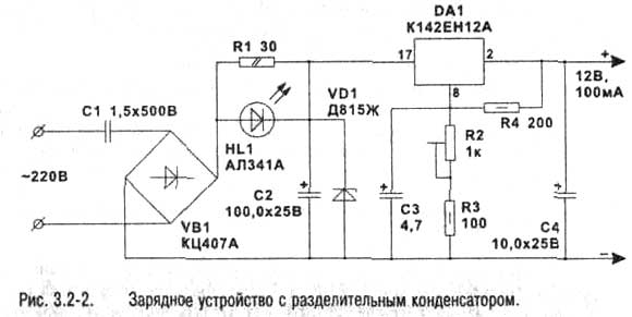
Thus, we choose C \u1,5d 500 μF with a double operating voltage of XNUMX V (capacitors of the following types can be used: MBM, MGBP, MBT). A complete diagram of a charger with a coupling capacitor is shown in fig. 3.2-2. The device is suitable for charging batteries with a current of not more than 100 mA at a charge voltage of not more than 15V. Trimmer resistor R2 set the required value of the charge voltage. R1 acts as a current limiter at the beginning of the charge, and the voltage generated on it is applied to the LED. By the intensity of the glow of the LED, you can judge how discharged the battery is.
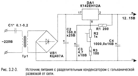
When operating this power supply (and any other power supply without galvanic isolation from the network), you must remember about safety measures. The device and the rechargeable battery are always under the potential of the industrial network. In some cases, such restrictions make normal operation of the devices impossible, so it is necessary to provide galvanic isolation of the IP from the network. A low-power power supply with a separating capacitor, but with galvanic isolation from the industrial network, can be made on the basis of a transition transformer or a magnetic starter relay, and their operating voltage can be lower than 220 V. In fig. 3.2-3 shows a schematic diagram of such a power supply. The capacitance of the isolation capacitor is calculated taking into account the parameters of the transformer (i.e., knowing the transformation ratio, first calculate the voltage that must be provided at the input of the transformer, and then, after making sure that such a voltage is acceptable for the transformer used, calculate the parameters of the capacitor). The power given off by such a power source may well feed a house bell, a receiver, an audio player.
4. Power supplies with coupling capacitors In micropower power supplies with galvanic coupling to an industrial network, so-called. coupling capacitors, which are nothing more than shunt resistors connected in series in the power circuit. It is known that a capacitor installed in an alternating current circuit has a resistance that depends on frequency and is called reactive. The capacitance of the isolation capacitor (assuming application in an industrial network ~ 220 V, 50 Hz) can be calculated using the following formula:
For example: a charger for 12V nickel-cadmium batteries with a capacity of 1 Ah can be powered from the mains through a separating capacitor. For nickel-cadmium batteries, the charging current is 10% of the nominal, i.e. 100 mA in our case. Further, taking into account the voltage drop across the stabilizer of the order of 3-5 V, we find that it is necessary to provide a voltage of ~ 18 V at the input of the charger at an operating current of 100 mA. Substituting this data, we get: according to the first formula:
Thus, we choose C \u1,5d 500 μF with a double operating voltage of XNUMX V (capacitors of the following types can be used: MBM, MGBP, MBT). A complete diagram of a charger with a coupling capacitor is shown in fig. 3.2-2. The device is suitable for charging batteries with a current of not more than 100 mA at a charge voltage of not more than 15V. Trimmer resistor R2 set the required value of the charge voltage. R1 acts as a current limiter at the beginning of the charge, and the voltage generated on it is applied to the LED. By the intensity of the glow of the LED, you can judge how discharged the battery is.
When operating this power supply (and any other power supply without galvanic isolation from the network), you must remember about safety measures. The device and the rechargeable battery are always under the potential of the industrial network. In some cases, such restrictions make normal operation of the devices impossible, so it is necessary to provide galvanic isolation of the IP from the network. A low-power power supply with a separating capacitor, but with galvanic isolation from the industrial network, can be made on the basis of a transition transformer or a magnetic starter relay, and their operating voltage can be lower than 220 V. In fig. 3.2-3 shows a schematic diagram of such a power supply. The capacitance of the isolation capacitor is calculated taking into account the parameters of the transformer (i.e., knowing the transformation ratio, first calculate the voltage that must be provided at the input of the transformer, and then, after making sure that such a voltage is acceptable for the transformer used, calculate the parameters of the capacitor). The power given off by such a power source may well feed a house bell, a receiver, an audio player.
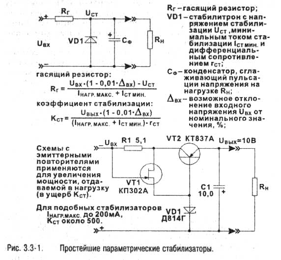
5. Linear power supplies Currently, traditional linear power supplies are increasingly being replaced by switching ones. However, despite this, they continue to be a very convenient and practical solution in most cases of amateur radio design (sometimes in industrial devices). There are several reasons for this: firstly, linear power supplies are structurally quite simple and easy to configure, secondly, they do not require the use of expensive high-voltage components, and, finally, they are much more reliable than pulsed power supplies. A typical linear power supply contains: a network step-down transformer, a diode bridge with a filter and a stabilizer that converts the unregulated voltage received from the secondary winding of the transformer through the diode bridge and filter into a stabilized output voltage, moreover, this output voltage is always lower than the unstabilized input voltage stabilizer. The main disadvantage of such a scheme is the low efficiency and the need to reserve power in almost all elements of the device (i.e., it requires the installation of components that allow higher loads than expected for the IP as a whole, for example, for a 10 W IP, a transformer with a power of at least 15 W is required and etc.). The reason for this is the principle by which the stabilizers of linear IPs function. It consists in dissipating some power on the regulating element Ppac = Iload * (Uin - Uout). It follows from the formula that the greater the difference between the input and output voltage of the stabilizer, the more power must be dissipated on the regulating element. On the other hand, the more unstable the input voltage of the regulator, and the more it depends on the change in load current, the higher it should be in relation to the output voltage. Thus, it can be seen that linear power supply stabilizers operate within a fairly narrow range of permissible input voltages, and these limits are even narrower when strict requirements are placed on the efficiency of the device. But the degree of stabilization and suppression of impulse noise achieved in linear IPs is much superior to other schemes. Let us consider in more detail the stabilizers used in linear IP. The simplest (so-called parametric) stabilizers are based on the use of the features of the current-voltage characteristics of some semiconductor devices - mainly zener diodes. They have a high output impedance. low level of stabilization and low efficiency. Such stabilizers are used only at low loads, usually as circuit elements (for example, as reference voltage sources). Examples of parametric stabilizers and formulas for calculation are shown in fig. 3.3-1.
Series pass-through linear stabilizers are distinguished by the following characteristics: the voltage at the load does not depend on the input voltage and load current, high values of the load current are allowed, a high stabilization coefficient and low output resistance are provided. The block diagram of a typical linear stabilizer is shown in fig. 3.3-2. The basic principle on which its work is based is to compare the output voltage with some stabilized reference voltage and control based on the results of this comparison, the main power element of the stabilizer (in the block diagram, the so-called pass-through transistor VT1, operating in linear mode, but it can also be a group of components), on which excess power is dissipated (see. formula above).
In most cases of amateur radio design, linear power supplies based on microcircuits of linear stabilizers of the K (KR) 142 series can be used as power sources for devices. They have very good parameters, have built-in overload protection circuits, thermal compensation circuits, etc., are easily accessible and easy to use (most of the stabilizers in this series are fully implemented inside the IC, which (have only three outputs). However, when designing linear IP high power (25-100 W), a more subtle approach is required, namely: the use of special transformers with armored cores (having a higher CDP), the direct use of only integral stabilizers is impossible due to their insufficient power, i.e. additional power components are needed and, as consequently, additional protection circuits against overload, overheating and overvoltage.Such IPs generate a lot of heat, require the installation of many components on large radiators and, accordingly, are quite large; special circuit solutions are required to achieve a high output voltage stabilization factor. 6. Stabilizer with load current up to 5A On fig. 3.3-3 shows the basic circuit for building powerful stabilizers that provide a load current of up to 5 A. which is quite enough to power most amateur radio designs. The circuit is made using a stabilizer chip of the KR142 series and an external pass transistor.
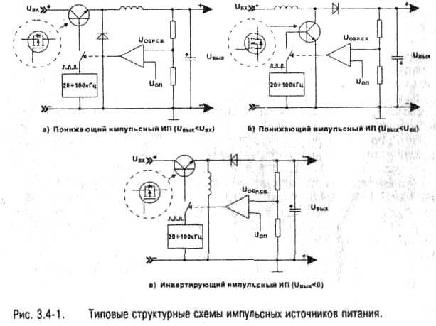
At low current consumption, transistor VT1 is closed and only the stabilizer microcircuit works, but with an increase in current consumption, the voltage allocated to R2 and VD5 opens transistor VT1, and the main part of the load current begins to flow through its junction. Resistor R1 serves as an overload current sensor. The greater the resistance R1, the lower the current protection is triggered (transistor VT1 closes). Filter choke L 1 serves to suppress AC ripple at maximum load. According to the above diagram, you can assemble stabilizers for a voltage of 5-15 V. The power diodes VD1-VD4 must be rated for a current of at least 10 A. Resistor R4 fine-tunes the output voltage (the base value is set by the type of stabilizer chip used series KR142). Power elements are installed on radiators with an area of at least 200 cm ^ 2. For example, let's calculate a voltage stabilizer with the following characteristics: Uout - 12 V; Ineg - 3A; Uin - 20 V. We choose a voltage stabilizer 12 V in the KR142 - KR142EN8B series. We select a pass-through transistor capable of dissipating the maximum load power Prac \u20d Uin * Iload \u3d 60 • 1.5 \u2d 818 W (it is advisable to choose a transistor power 100-15 times greater) - the common KT1A is suitable (Rrac \u5d 202 W, Ik max \uXNUMXd XNUMX A). As VDXNUMX-VDXNUMX, any suitable power diodes can be used, for example, KDXNUMXD. 7. Switching power supplies Unlike traditional linear power supplies, which assume the damping of excessive unstabilized voltage on a linear through element, pulsed power supplies use other methods and physical phenomena to generate a stabilized voltage, namely: the effect of energy accumulation in inductors, as well as the possibility of high-frequency transformation and the conversion of stored energy into constant pressure. There are three typical schemes for constructing pulsed power supplies (see Fig. 3.4-1): step-up (output voltage is higher than input), step-down (output voltage is lower than input) and inverting (output voltage has the opposite polarity with respect to the input). As can be seen from the figure, they differ only in the way of connecting the inductance, otherwise, the principle of operation remains unchanged, namely. A key element (usually bipolar or MIS transistors are used), operating at a frequency of about 20-100 kHz, periodically for a short time (no more than 50% of the time) applies the full input unstabilized voltage to the inductor. impulse current. flowing through the coil, ensures the accumulation of energy in its magnetic field 1/2LI^2 on each pulse. The energy stored in this way from the coil is transferred to the load (either directly, using a rectifying diode, or through the secondary winding and then rectified), the output smoothing filter capacitor ensures that the output voltage and current are constant. Stabilization of the output voltage is provided by automatic adjustment of the width or frequency of the pulses on the key element (the feedback circuit is designed to monitor the output voltage).
This, although rather complex, scheme can significantly increase the efficiency of the entire device. The fact is that, in this case, in addition to the load itself, there are no power elements in the circuit that dissipate significant power. Key transistors operate in a saturated key mode (i.e., the voltage drop across them is small) and dissipate power only in fairly short time intervals (the time of the pulse). In addition, by increasing the conversion frequency, it is possible to significantly increase the power and improve the weight and size characteristics. An important technological advantage of pulsed IP is the possibility of building on their basis small-sized network IP with galvanic isolation from the network to power a wide variety of equipment. Such IPs are built without the use of a bulky low-frequency power transformer according to the high-frequency converter circuit. This, in fact, is a typical circuit of a pulsed power supply with a voltage reduction, where a rectified mains voltage is used as an input voltage, and a high-frequency transformer (small-sized and with high efficiency) is used as a storage element, from the secondary winding of which the output stabilized voltage is removed (this transformer also provides galvanic isolation from the network). The disadvantages of pulsed power supplies include: the presence of a high level of impulse noise at the output, high complexity and low reliability (especially in handicraft production), the need to use expensive high-voltage high-frequency components, which, in the event of the slightest malfunction, easily fail "en masse" (with this, as a rule, one can observe impressive pyrotechnic effects). Those who like to delve into the insides of devices with a screwdriver and a soldering iron will have to be extremely careful when designing a network pulsed IP, since many elements of such circuits are under high voltage. 8. Efficient Low Complexity Switching Regulator On the element base, similar to that used in the linear stabilizer described above (Fig. 3.3-3), you can build a switching voltage regulator. With the same characteristics, it will have significantly smaller dimensions and better thermal conditions. A schematic diagram of such a stabilizer is shown in fig. 3.4-2. The stabilizer is assembled according to a typical scheme with a voltage drop (Fig. 3.4-1a). When first turned on, when the capacitor C4 is discharged and a sufficiently powerful load is connected to the output, the current flows through the linear regulator IC DA1. The voltage drop across R1 caused by this current unlocks the key transistor VT1, which immediately enters saturation mode, since the inductive resistance L1 is large and a sufficiently large current flows through the transistor. The voltage drop across R5 opens the main key element - transistor VT2. Current. increasing in L1, charges C4, while the stabilizer and the key transistor are locked through the feedback on R8. The energy stored in the coil powers the load. When the voltage at C4 drops below the stabilization voltage, DA1 and the key transistor open. The cycle is repeated at a frequency of 20-30 kHz.
Chain R3. R4, C2 will set the output voltage level. It can be smoothly adjusted within a small range, from Uct DA1 to Uin. However, if Uout is raised close to Uin, there is some instability at maximum load and an increased level of ripple. To suppress high-frequency ripples, a filter L2, C5 is included at the output of the stabilizer. The scheme is quite simple and most effective for this level of complexity. All power elements VT1, VT2, VD1, DA1 are supplied with small radiators. The input voltage must not exceed 30 V, which is the maximum for KR142EN8 stabilizers. Rectifier diodes should be used for a current of at least 3 A. 9. Uninterruptible power supply device based on a switching regulator On fig. 3.4-3, a device for uninterruptible power supply of security and video surveillance systems based on a switching stabilizer combined with a charger is proposed for consideration. The stabilizer includes protection systems against overload, overheating, output surges, short circuits. The stabilizer has the following parameters:
The principle of operation of the switching stabilizer in the described device is the same as that of the stabilizer presented above. The device is supplemented with a charger made on the elements DA2, R7, R8, R9, R10, VD2, C7. Voltage regulator IC DA2 with current divider on R7. R8 limits the maximum initial charge current, the divider R9, R10 sets the charge output voltage, the VD2 diode protects the battery from self-discharge in the absence of supply voltage. Overheating protection uses thermistor R16 as a temperature sensor. When the protection is triggered, the sound signaling device assembled on the IC DD 1 is turned on and, at the same time, the load is disconnected from the stabilizer, switching to battery power. The thermistor is mounted on the radiator of the transistor VT1. Precise adjustment of the level of operation of the temperature protection is carried out by the resistance R18. The voltage sensor is assembled on a divider R13, R15. resistance R15 sets the exact level of operation of overvoltage protection (13 V). When the voltage at the output of the stabilizer is exceeded (in the event of the failure of the last one), relay S1 disconnects the load from the stabilizer and connects it to the battery. In the event of a power failure, relay S1 goes into the "default" state - i.e. connects the load to the battery. The circuit shown here does not have electronic short circuit protection for the battery. this role is performed by a fuse in the load power circuit, designed for the maximum current consumption.
10. Power supplies based on a high-frequency pulse converter Quite often, when designing devices, there are strict requirements for the size of the power source. In this case, the only way out is to use a power supply based on high-voltage high-frequency pulse converters. which are connected to the ~220 V network without the use of an overall low-frequency step-down transformer and can provide high power with small dimensions and heat dissipation. The block diagram of a typical pulse converter powered by an industrial network is shown in Figure 34-4.
The input filter is designed to prevent the penetration of impulse noise into the network. Power switches provide high voltage pulses to the primary winding of a high-frequency transformer (one- and two-cycle circuits can be used). The frequency and duration of the pulses are set by a controlled generator (usually, pulse width control is used, less often - frequency). Unlike low-frequency sine-wave transformers, pulsed power supplies use wideband devices to provide efficient power transfer on signals with fast edges. This imposes significant requirements on the type of magnetic circuit used and the design of the transformer. On the other hand, with increasing frequency, the required dimensions of the transformer (while maintaining the transmitted power) decrease (modern materials make it possible to build powerful transformers with acceptable efficiency at frequencies up to 100-400 kHz). A feature of the output rectifier is the use of not ordinary power diodes, but high-speed Schottky diodes, which is due to the high frequency of the rectified voltage. The output filter smoothes the output voltage ripple. The feedback voltage is compared with the reference voltage and then controls the generator. Pay attention to the presence of galvanic isolation in the feedback circuit, which is necessary if we want to provide isolation of the output voltage from the network. In the manufacture of such IP, there are serious requirements for the components used (which increases their cost compared to traditional ones). Firstly, it concerns the operating voltage of the rectifier diodes, filter capacitors and key transistors, which should not be less than 350 V in order to avoid breakdowns. Secondly, high-frequency key transistors (operating frequency 20-100 kHz) and special ceramic capacitors should be used (ordinary oxide electrolytes will overheat at high frequencies due to their high inductance). And thirdly, the saturation frequency of a high-frequency transformer, determined by the type of magnetic circuit used (as a rule, toroidal cores are used) must be significantly higher than the operating frequency of the converter.
On fig. 3.4-5 shows a schematic diagram of a classic IP based on a high-frequency converter. The filter, consisting of capacitors C1, C2, C3 and chokes L1, L2, serves to protect the power supply from high-frequency interference from the converter. The generator is built according to a self-oscillating circuit and is combined with a key stage. The key transistors VT1 and VT2 operate in antiphase, opening and closing in turn. Starting the generator and reliable operation is ensured by the VT3 transistor, which operates in the avalanche breakdown mode. When the voltage on C6 rises through R3, the transistor opens and the capacitor is discharged to the base of VT2, starting the generator. The feedback voltage is removed from the additional (III) winding of the power transformer Tpl. Transistors VT1. VT2 is installed on plate radiators of at least 100 cm ^ 2. Diodes VD2-VD5 with a Schottky barrier are placed on a small radiator 5 cm ^ 2. Choke and transformer data: L1-1. L2 is wound on rings made of ferrite 2000NM K12x8x3 in two wires with a PELSHO 0,25 wire: 20 turns. TP1 - on two rings put together, ferrite 2000NN KZ 1x18.5x7; winding 1 - 82 turns with wire PEV-2 0,5: winding II - 25 + 25 turns with wire PEV-2 1,0: winding III - 2 turns with wire PEV-2 0.3. TP2 is wound on a ferrite ring 2000NN K10x6x5. all windings are made with PEV-2 0.3 wire: winding 1 - 10 turns: windings II and III - 6 turns each, both windings (II and III) are wound so that they occupy 50% of the area on the ring without touching or overlapping each other, winding I is wound evenly over the entire ring and insulated with a layer of varnished cloth. Rectifier filter coils L3, L4 are wound on ferrite 2000NM K 12x8x3 with PEV-2 1,0 wire, the number of turns is 30. KT1A can be used as key transistors VT2, VT809. KT812, KT841. The ratings of the elements and the winding data of the transformers are given for an output voltage of 35 V. In the case when other operating parameters are required, the number of turns in the winding 2 Tr1 should be changed accordingly. The described circuit has significant drawbacks due to the desire to minimize the number of components used. This is a low "level of output voltage stabilization, and unstable unreliable operation, and low output current. However, it is quite suitable for powering the simplest structures of different power (when using appropriate components), such such as: calculators, callers, lighting fixtures, etc.
Another IP circuit based on a high-frequency pulse converter is shown in fig. 3.4-6. The main difference between this circuit and the standard structure shown in Fig. 3-4 is the lack of a feedback loop. In this regard, the voltage stability at the output windings of the RF transformer Tr4 is quite low and the use of secondary stabilizers is required (the circuit uses universal integrated stabilizers on the KR2 series ICs). 11. Switching regulator with a key MIS transistor with current sensing Miniaturization and increase in efficiency in the development and design of switching power supplies is facilitated by the use of a new class of semiconductor inverters - MOS transistors, as well as: high-power diodes with fast reverse recovery, Schottky diodes, ultra-fast diodes, field-effect transistors with an insulated gate, integrated circuits for controlling key elements. All these elements are available on the domestic market and can be used in the design of high-efficiency power supplies, converters, ignition systems for internal combustion engines (ICE), fluorescent lamp start systems (LDS). Of great interest to developers can also be a class of power devices called HEXSense - MIS transistors with current sensing. They are ideal switching elements for ready-to-operate switching power supplies. The ability to read the current of the switching transistor can be used in pulsed power supplies for the current feedback required by the PWM controller. This achieves a simplification of the design of the power supply - the exclusion of current resistors and transformers from it. On fig. 3.4-7 shows a diagram of a 230 W switching power supply. Its main performance characteristics are as follows:
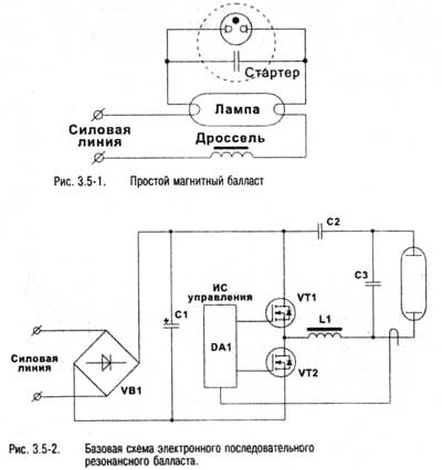
The circuit is based on a pulse-width modulator (PWM) with a high-frequency converter at the output. The principle of operation is as follows. The key transistor control signal comes from output 6 of the PWM controller DA1, the duty cycle is limited to 50% by resistor R4, R4 and C3 are the timing elements of the generator. Power supply DA1 is provided by the chain VD5, C5, C6, R6. Resistor R6 is designed to supply voltage during the start of the generator, subsequently, voltage feedback is activated through L1, VD5. This feedback is obtained from an additional winding in the output choke, which operates in flyback mode. In addition to powering the generator, the feedback voltage through the chain VD4, Cl, Rl, R2 is fed to the voltage feedback input DA1 (pin 2). Through R3 and C2 a compensation is provided which guarantees the stability of the feedback loop. As a key element of VT2, an MIS transistor with current sensing IRC830 from International Rectifier is used. The current reading signal is supplied from VT2 to pin 3 of DA1. The voltage level at the current sense pin is set by resistor R7 and is proportional to the drain current, C9 suppresses spikes on the rising edge of the drain current pulse that can cause premature controller operation. VT1 and R5 are used to set the required control law. Note that the read current is returned to the crystal at the source pin. This is done for that. to avoid a current reading error that can occur due to a voltage drop across the parasitic resistance of the source pin. On the basis of this scheme, it is possible to build switching stabilizers with other output parameters. 12. Modern gas discharge devices Approximately 25% of the electricity generated in the world is consumed by artificial lighting systems, which makes this area extremely attractive for efforts to improve efficiency and reduce electricity consumption. Currently, the most common economical light sources are gas discharge lamps, which are increasingly being used instead of conventional incandescent lamps. The principle of operation of such lamps is the luminescent glow of the gas enclosed inside the lamp when current flows through it (high-voltage breakdown), which is ensured by applying high voltage to the lamp electrodes. Discharge lamps can be divided into two types, the first is high intensity lamps, among which the most common are mercury lamps, high pressure sodium lamps and metal halide lamps, the second is low pressure fluorescent lamps. Low pressure lamps are used for lighting in most cases of everyday life - in administrative buildings, offices, residential buildings: they are distinguished by rich white light. close to daylight (hence the name - "fluorescent lamps"). High pressure lamps are used for outdoor lighting - in street lamps, spotlights, etc. If a conventional incandescent lamp, when turned on, is a constant resistive load, then all gas discharge lamps have negative impedance characteristics. that require current stabilization. In addition, it is necessary to take into account such moments as: resonant mode of operation, protection in case of lamp failure; high voltage ignition, special power bus control. The main mode, which is necessary for a fluorescent lamp to be observed throughout the entire period of operation, is the current mode (ideally, power stabilization is necessary throughout the entire period of operation of the lamp). As a rule, lamps are powered by alternating voltage to equalize the wear of the electrodes (in the case of a direct voltage supply, the service life is reduced by 50%). 13. Magnetic and electronic ballasts To control gas-discharge lamps, the so-called. magnetic ballast (see the diagram in Fig. 3.5-1), however, due to its inefficiency and unreliability, recently electronic control circuits have become more widespread - electronic ballast, which can significantly increase the efficiency and service life of lighting systems, make the light more even and natural to the eyes.
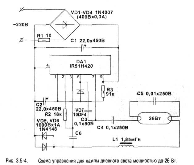
The basic circuit of an electronic ballast with series resonance is shown in fig. 3.5-2. Using electronic ballasts, you can control lamps of any power, any additional devices can be built into the circuit (for example, a photorelay that turns on lighting at dusk and turns off at dawn). 14. Control circuit for a fluorescent lamp with a power of up to 40W To control a fluorescent lamp (LDS) with a power of up to 40 W, the circuit shown in fig. 3.5-3. Supply voltage ~220 V is applied to inputs L1 and L2. The DC voltage rectified by diodes VD1 -VD4 is about 320 V. Capacitors C1 and C2 work as a capacitive input filter. It is also possible to use a ~ 110V network, in this case, power is supplied to the inputs L1 (L2) and N. and the diodes VD1. VD3 (VD2, VD4) with capacitors C1 and C2 work as a half-wave voltage doubler. DA1 (IR2151) is an MIS transistor driver circuit with an internal oscillator that runs directly from the power rail through R1. The internal regulator fixes the supply voltage at 15 V. The gates are blocked when the supply voltage drops below 9 V. With a nominal 230V DC supply voltage, the output square wave has an effective voltage of 160V, and the frequency is set by adjusting R2 and C4 to approximate the resonant frequency of the tube. The lamp operates in its series resonant circuit, consisting of a series-connected inductor L1 and a shunt capacitor C6, which is in parallel with the PTC thermistor. The thermistor (a neon light can also be used for this purpose) has a low resistance when cold and a very high resistance when hot, when heated by the current flowing through it. The purpose of the thermistor is to provide a smooth increase in voltage at the lamp electrodes when turned on. In cases where the lamp is constantly on or very rarely turns on / off, the thermistor can be removed. In this case, the lamp turns on instantly, which can lead to its rapid wear. 15. Subminiature control circuit for fluorescent lamp up to 26W The following schematic diagram, shown in fig. 3.5-4, allows you to control a fluorescent lamp (LDS), while having subminiature dimensions, since it does not use power inverters (IC IR51H420 combines IC IR2151 and MIS keys in one package). The maximum lamp power in this case should not exceed 26 W, which is quite enough to illuminate one workplace.
16. Boost converters and voltage multipliers Usually, if the design has mains power, transformers are used to receive all the supply voltages. Boost converters and voltage multipliers are used when it is necessary to obtain voltages greater than the supply voltages in portable devices powered by batteries or accumulators. Low power converters (up to 100-200 mW) can be assembled on discrete elements without the use of transformers; in high power converters, a transformer is required. To obtain a double or triple voltage, you can use the so-called. voltage multipliers (see chapter 2). 17. Transformerless voltage doubler for small devices On fig. 3.6-1 shows a diagram of a voltage converter 9 V -> 18V for devices that consume no more than 100 mA at a supply voltage of 18V. The converter is included in the practical siren circuit for security and alarm systems. The control generator is made according to a typical scheme. At the output D 1.2 rectangular pulses are formed with a frequency of 1 Hz. The pulses are fed to the controlled generator Dl.3, D1.4 and a chain of R3, R2, C2, which affects the modulation depth. R4, R5, C3, C4 are selected in accordance with the resonant frequency of the piezo ceramic emitter B 1 within 1,5-3 kHz. To increase the amplitude on the piezocrystal, a multiplier is introduced into the circuit. The signal from the output DD1.4 goes to the complementary pair VT5, VT6 and then to the multiplier VD3, VD4, C5, Sat. The voltage on C6 at a load current of 50 mA and a main power supply of 9 V is about 16 V. The power of the multiplier can be slightly increased by using larger capacitances. The circuit can be powered with 6-15V (15V maximum for 561 series ICs), in case of 15V supply, the voltage at the output of the multiplier will be less than 25V at 80mA load.
18. Powerful converter for powering household appliances On fig. 3.6-2 shows a schematic diagram of a powerful converter for powering household electrical appliances (TV, drill, electric pump, etc.) from a car battery. The converter provides an output voltage of 220 V, 50 Hz at a load of up to 100 W. At maximum load, the current consumed from the battery does not exceed 10 A. The number of parts in the device is kept to a minimum. A master oscillator with a frequency of 1.1 Hz is assembled on the DD100 chip. Fine-tuning the frequency (which is important for the normal operation of the equipment) is carried out by resistors R1 and R2. Frequency division by 2 and transistor control are provided by the second half of the microcircuit - D1.2. Transistors VT1, VT2 are included to ensure the normal operation of the outputs DD1.2 at maximum load current. Output transistors VT3, VT4 are installed on radiators with an area of at least 350 cm ^ 2. Capacitor C3 is designed to smooth rectangular fronts, which, together with the output winding and load, forms a resonant system. Its capacity is highly dependent on the nature of the load. Transformer TP1 is made on the magnetic circuit of the ShLM or PLM brand with an overall power of 100 W. Windings I and II contain 17 turns of PEV-2 wire 2,0 mm each, winding III contains 750 turns of PEV-2 wire 0,7 mm. This circuit is very easy to rework for a high-frequency voltage converter (conversion frequency ~ 25 kHz). To do this, it is enough to raise the frequency of the master oscillator by D1.1 to -50 kHz, changing the capacitances C1 and C2 by 180 pF, and replace TR1 with a high-frequency transformer. The power of the converter depends on the load of the output transistors, the maximum current that they can give should not exceed 8A in the arm. To increase the current, the number of turns of the transformer in the 1st and 8nd windings is reduced to 10-25. A diode bridge and an RF filter are installed at the output of the converter, the components used in them must ensure normal operation at a frequency of XNUMX kHz.
19. Over voltage protection In an industrial and domestic network, it is quite often possible to fix unforeseen voltage surges, while the voltage in the network can exceed the nominal voltage by 20-40%. Such throws can be conditionally divided into two classes: 1. Short-term - an increase in amplitude over several periods. 2. Long-term - an increase in voltage for several seconds or minutes. The former can be attributed rather to impulse noise, which is associated with the switching of some powerful loads on the line (welding machines, motors, heating elements). They undoubtedly have an impact on household appliances and, especially, on sensitive elements of power supplies for TVs and audio centers. which are often on standby around the clock. 20. Network surge protection device The device that protects against impulse noise is shown in fig. 3.7-1. The scheme consists of the following nodes:
The power supply produces two voltages: +24V to power the pulse transformer, +5V to power the device IC.
The voltage control unit is assembled on Rl, R2, R3. From the divider, the voltage is fed to the input of the comparator. The overvoltage response level is set by resistor R2 (the position of the slider is selected so that the comparator is on the verge of triggering at 245 V at the input). When the comparator input exceeds the specified amplitude value, it switches and rectangular pulses with a frequency of 25 Hz appear at the output. In the initial state, the output D1.2 is maintained at a high logic level, allowing the operation of the triac control generator (to keep it open). Transistor VT1 controls the pulse transformer. forming powerful voltage pulses open. The generator frequency is chosen equal to 25 kHz for the fastest unlocking of the power switch at the moments of transition through "zero" (if the control frequency is insufficient, it may happen that when high-voltage surges appear during switching on and the shape of the sinusoidal signal is distorted, the system will not have time to react and distorted the signal will go to the load). The differentiating circuit on the elements D1.1 and D1.2 prohibits the operation of the generator when a low level is received from the output of the comparator (when the threshold voltage in the network rises) and, with a delay of 9 seconds, allows the generator to start when the voltage drops to a threshold value of 240 V. The pulse transformer TP1 is wound on a matt core of size K20x10x7,5 made of ferrite grade 2000NN and contains: winding I - 100 turns, winding II - 40 turns of PELSHO-0,22 wire. The windings are isolated from the ring with a layer of varnished cloth and placed on opposite sides of the ring. With a load power of more than 300 W, the triac must be installed on a radiator. Publication: cxem.net
Machine for thinning flowers in gardens
02.05.2024 Advanced Infrared Microscope
02.05.2024 Air trap for insects
01.05.2024
▪ Creative Sound Blaster Series Headsets ▪ Electric vehicle chargers from McDonald's ▪ External optical drives Buffalo BRXL-PC6VU2-C
▪ site section Color and music installations. Selection of articles ▪ article Wise minnow. Popular expression ▪ article Is the New Year celebrated in the same way all over the world? Detailed answer ▪ article Lying fenugreek. Legends, cultivation, methods of application ▪ Article Rubber glue. Simple recipes and tips ▪ article Invulnerable tapes. Focus Secret
Home page | Library | Articles | Website map | Site Reviews
www.diagram.com.ua |


 Leave your comment on this article: