|
|


 Arabic
 Bengali
 Chinese
 English
 French
 German
 Hebrew
 Hindi
Hindi Italian
 Japanese
 Korean
 Malay
Malay Polish
 Portuguese
 Spanish
 Turkish
 Ukrainian
 Vietnamese
|
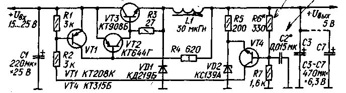
ENCYCLOPEDIA OF RADIO ELECTRONICS AND ELECTRICAL ENGINEERING Improving the switching voltage stabilizer. Encyclopedia of radio electronics and electrical engineering
Encyclopedia of radio electronics and electrical engineering / Surge Protectors In the magazine "Radio" No. 8 for 1985, in the article "A simple key voltage stabilizer", a switching voltage regulator was described, which, with the relative simplicity of the technical solution, has high energy performance and is quite suitable for powering devices on TTL microcircuits. At the same time, with further refinement of the stabilizer, such characteristics as efficiency, instability of the output voltage, duration and nature of the transient process when exposed to a pulsed load were significantly improved. It has been established that during the operation of the stabilizer, the so-called through current occurs through a composite key transistor. This current appears at those moments when, at the signal of the comparison node, the key transistor opens, and the switching diode has not yet had time to close. The presence of this current causes additional losses for heating the transistor and diode and reduces the efficiency of the entire device. Another disadvantage is a significant ripple of the output voltage at a load current close to the limit. To combat ripple, an additional output LC filter (L2C6) was introduced into the stabilizer. It is possible to reduce the instability of the output voltage from a change in the load current only by reducing the active resistance of the inductor L2. Improving the dynamics of the transient process (in particular, reducing its duration) is associated with the need to reduce the inductance of the inductor, but this will inevitably increase the output voltage ripple.
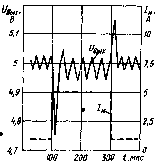
Therefore, it turned out to be advisable to exclude the L2C6 filter (Fig. 1), and increase the total capacitance of the capacitors C3, C4 by 5 ... 10 times by connecting several capacitors in parallel to the battery. On fig. 2 shows a view of the transient process in the modified stabilizer with a pulsed load. Comparison with the graph presented in fig. 3a in the above article shows a significant improvement in the transient.
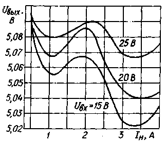
Load characteristics Uout=f(In) (see also Fig. 2, b of the same article) for different values of the input voltage of the modified stabilizer are shown in fig. 3. From the comparison of these figures, it can be seen that the instability of the output voltage in the output current range from 0,5 to 4 A at an input voltage of 15 ... 25 V decreased by 2 times.
The R3C2 circuit in the original stabilizer practically does not change the duration of the output current decline, so it can be removed (close the resistor R3), and the resistance of the resistor R4 can be increased to 820 ohms. But then, with an increase in the input voltage from 15 V to 25 V, the current flowing through the resistor R4 (in the original device) will increase by 1,7 times, and the dissipation power will increase by 3 times (up to 0,7 W). By connecting the lower resistor R4 according to the output circuit (it is also R4 on the circuit of the modified stabilizer) to the positive terminal of the capacitors C3, C4, this effect can be weakened, but its resistance should be reduced to 620 ohms. One of the effective ways to combat the through current is to increase the rise time of the current through the opened key transistor. Then, when the transistor is fully opened, the current through the VD1 diode will decrease to almost zero. This can be achieved if the shape of the current through the key transistor is close to triangular. As the calculation shows, to obtain such a form of current, the inductance of the storage inductor L1 should not exceed 30 μH. Another way is to use a faster switching diode (VD1), for example, KD219B. This is the so-called Schottky barrier diode. Such diodes have higher speed and less voltage drop at the same current value compared to conventional high-frequency silicon. Capacitors C3-C7 - from the K52-1 series. All of the above changes do not lead to a significant change in the circuit diagram and printed circuit board of the stabilizer. An improvement in the parameters of the device can also be obtained by changing the operating mode of the key transistor. The peculiarity of the operation of the powerful transistor VT3 in the original and improved stabilizers is that it operates in the active mode, but in the unsaturated mode, and therefore has a high current transfer coefficient and closes quickly. However, due to the increased voltage on it, when it is open, the power dissipation is 1,5 ... 2 times the minimum achievable value. You can lower the voltage on the key transistor by applying a positive bias voltage relative to the positive power wire to the emitter of the transistor VT2 (see Fig. 1). The value of the bias voltage is selected when adjusting the stabilizer. If it is powered by a rectifier connected to a mains transformer, then a separate winding on the transformer can be provided to obtain the bias voltage. However, in this case, the bias voltage will change along with the mains voltage. To obtain a stabilized bias voltage, the stabilizer must be modified (Fig. 4), and the inductor must be turned into a transformer T1 by winding an additional winding II. When the key transistor is closed and the VD1 diode is open, the voltage on winding 1 is determined from the expression: U1==Uout+Uvd1. Since the voltage at the output and across the diode at this time changes slightly, then regardless of the value of the input voltage on winding II, the voltage is practically stabilized. After rectification, it is fed to the emitter of the transistor VT2.
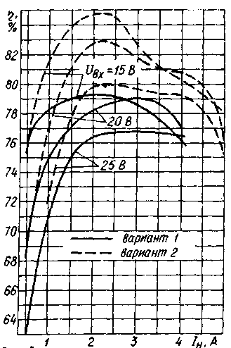
The improvement of the energy characteristics of the second version of the modified stabilizer is illustrated in Fig. 5, where, for comparison, similar dependencies are shown for the first variant (compare also with Fig. 2a in the article mentioned above). At the same time, heating losses decreased in the first version of the modified stabilizer by 14,7%, and in the second - by 24,2%, which allows them to operate at a load current of up to 4 A without installing a key transistor on the heat sink.
In the stabilizer of option 1, the L1 choke contains 11 turns wound with a bundle of eight PEV-1 0,35 conductors. The winding is placed in the B22 armored magnetic circuit made of 2000NM ferrite. Between the cups you need to lay a gasket made of textolite with a thickness of 0,25 mm. In the stabilizer of option 2, the transformer T1 is formed by winding two turns of wire PEV-1 1 over the inductor coil L0.35. Instead of a germanium diode D310, you can use silicon, for example, KD212A or KD212B, while the number of turns of winding II must be increased to three. Author: A. Mironov, Lyubertsy, Moscow Region; Publication: N. Bolshakov, rf.atnn.ru
Artificial leather for touch emulation
15.04.2024 Petgugu Global cat litter
15.04.2024 The attractiveness of caring men
14.04.2024
▪ New opportunities for overclocking 7nm chips ▪ Samsung Exynos ModAP processor with LTE modem ▪ SSDs have no future, scientists say
▪ section of the site Tools and mechanisms for agriculture. Article selection ▪ article King Lear. Popular expression ▪ article Operator of the recipient station. Standard instruction on labor protection
Home page | Library | Articles | Website map | Site Reviews
www.diagram.com.ua |


 Leave your comment on this article: