|
|


 Arabic
 Bengali
 Chinese
 English
 French
 German
 Hebrew
 Hindi
Hindi Italian
 Japanese
 Korean
 Malay
Malay Polish
 Portuguese
 Spanish
 Turkish
 Ukrainian
 Vietnamese
|
ENCYCLOPEDIA OF RADIO ELECTRONICS AND ELECTRICAL ENGINEERING Resettable electronic fuse
Encyclopedia of radio electronics and electrical engineering / Protection of equipment from emergency operation of the network The proposed electronic fuse monitors the load resistance. It not only turns it off in case of overload, but also restores itself to its original mode when the load resistance returns to normal. The high-speed electronic fuse described in article [1] automatically connects the load at the moment of power-up if there is no short circuit or overload in it. In the event of an overload, the fuse disconnects the load. To turn it on again, you must press the "Start" button of the fuse or turn the power off and on again, which is not always convenient. The proposed device, developed on the basis of the previous one, is fully automatic. It has no governing bodies. The device determines the serviceability of the load by its resistance. If it is greater than the allowable limit, the load is automatically connected to the power source. Otherwise, the device disconnects the load according to its fuse function. For a short time (about 10 µs), the load is periodically connected to the power source through current-limiting resistors. During this time, the electronic fuse measures the load resistance and, if it has returned to the permissible limit, it itself recovers from the state of emergency load shutdown to normal. An electronic fuse is connected between the power supply and the load. The device is operable at a voltage of 12 to 30 V and a load current of up to 20 A. Two versions of the device have been developed: with switching of the negative or positive wire of the load power supply. The scheme of the first variant is shown in fig. 1, the second - in Fig. 2. Components that perform the same function are labeled the same.
The device (see Fig. 1) has two load control circuits: preliminary (on the DA3 comparator) and main (on the DA4 comparator). The load resistance is measured when it is connected by the transistor VT1 through resistors R2 and R3. If the load resistance is greater than the operating threshold set by the tuning resistor R7, the main switching transistor VT2 opens, which connects the load to the power source. The load current in normal mode monitors the main circuit on the comparator DA4. If it exceeds the response threshold set by the trimmer resistor R14, the main switching transistor VT2 will close. The preliminary circuit based on the DA3 comparator comes into operation, which will allow the main switching field-effect transistor VT2 to be reopened when the load resistance returns to the permissible limit. To control the transistor VT2, as in the previous device [1], an RS flip-flop was used on elements DD1.2 and DD1.3. The advantage of such a flip-flop is that it allows the logically simultaneous presence of active control signals on both control inputs. The control signal that directly affects the output used [2] dominates. In our case, the used direct output of the RS flip-flop (pin 3 DD1) is dominated by an active high-level signal at the installation input S (pin 1 DD1). For an RS flip-flop made on OR-NOT elements, the active level of the direct output signal is low, therefore, an inverter on the DD2 element is used to control the transistor VT1.4. Input R RS-flip-flop (pin 8 DD1) is connected to the output of the comparator DA4 (pin 9 - open collector). At the time of power-up and during transients, the transistor VT2 is closed, since the R1C2 circuit provides the supply voltage through the DA1 stabilizer to the DD1 and DA2 microcircuits later than to the comparators DA3 and DA4. The voltage at the non-inverting input (pin 3) of the DA4 comparator is greater than the voltage at its inverting input (pin 4), so the output transistor of the comparator (pins 2 and 9) is closed. As soon as power is supplied to the DD1 chip, a high level from the DA4 output (pin 9) will set the RS flip-flop to a high level state at pin 3 of DD1. The output of the inverter DD1.4 and the gate of the transistor VT2 is low, so it is closed. In this state, the transistor VT2 will be until the upper input of the DD1.2 element in the circuit receives a triggering short high-level pulse. It is generated at the output of the element DD1.1 when low-level pulses appear simultaneously at its inputs. Triggering pulses are received at the upper input of the DD1.1 element according to the circuit - short pulses of a low level of high duty cycle, which are generated by the generator on the DA2 timer, resistors R4, R5 and capacitor C4. The pulse duration is equal to R5C4ln2 ~ 25 µs, and their repetition period is (R4+2R5)C4ln2 = 2 ms [3]. After energizing the timer DA2, the first pulse at its output 3 appears with a delay (R4+R5)C4ln2 = 2 ms for the duration of the transients of the initial installation of the RS flip-flop DD1.2, DD1.3. Each trigger pulse from output 3 of the DA2 timer goes to the upper input of the DD1.1 element according to the circuit and, at the same time, through the inverter on the transistor VT3 already in the form of a short high-level pulse - to the gate of the transistor VT1, which, opening, connects the load to the power source through resistors R2 and R3. They not only limit the load current, but also form a circuit for measuring its resistance: the connection point of these resistors is connected to the non-inverting input (pin 3) of the DA3 comparator. The circuit R4-R6 is connected to the inverting input (pin 8) of this comparator. The position of the trimmer resistor R7 determines the load resistance at which the comparator DA3 switches. After the power is turned on, the transistor VT1 is closed, so the voltage at the non-inverting input of the comparator DA3 will always be greater than the voltage at its inverting input, so the output transistor of the comparator (pins 2 and 9) is closed. A single signal at the lower input of the element DD1.1 according to the circuit provides a low level at its output and, accordingly, at the input S of the RS flip-flop, which will thus retain its original state. If, with the open transistor VT1, the load resistance is less than the permissible limit, then the voltage at the non-inverting input of the comparator DA3 will be greater than the voltage at its inverting input. At the output (pin 9) of the comparator DA3, the same state will remain that was when the transistor VT1 was closed. A high level from the output of the comparator DA3, going to the lower input of the element DD1.1, blocks the passage of trigger pulses from the output of the timer DA2 until the overload of the electronic fuse output disappears. If, with the open transistor VT1, the load resistance is greater than the permissible limit, then the voltage at the inverting input of the comparator DA3 will be greater than the voltage at its non-inverting input. The output transistor of the comparator DA3 (pins 2 and 9) is open. At the inputs of the element DD1.1 there will be overlapping (with a slight shift) in time short low-level pulses. At the output of this element, a short high-level pulse will be generated, which will switch the RS-flip-flop at the input S to a state with a low level at the output. By this time, there is already a high level at the input R from the comparator DA4. But the signal at the input S has a higher priority, so the output of the trigger is low. As a result, a single signal from the output of the inverter DD1.4 will open the transistor VT2. If the load current is less than the protection operation limit, the DA4 comparator will go into a stable state with a low output level. An open transistor VT2 sets a small (fraction of a volt) voltage at the non-inverting input of the comparator DA3, regardless of the state of the transistor VT1. The voltage at the inverting input DA3 is close to about half the input voltage. Since the pin 9 of the comparator DA3 has a stable low level, the triggering pulses from the output of the timer DA2 through the element DD1.1 save the current state of the RS flip-flop. If the load current exceeds the allowable limit, the DA4 comparator switches so that its output transistor closes. A single signal will set a high level at the output of the trigger and, accordingly, a low level at the output of the inverter DD1.4, as a result of which the transistor VT2 will close and turn off the load.
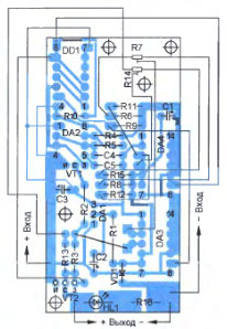
An electronic fuse with positive wire switching works similarly (Fig. 2). It is distinguished by the use of p-channel transistors VT1 and VT2. Since the control signals must be applied to the gates of the transistors with respect to their sources connected to the positive power wire, they are inverted. Therefore, inverters on the element DD1.4 and transistor VT3 are not used. Construction and details. The electronic fuse is made by surface mounting on a printed circuit board measuring 35x70 mm from double-sided foil fiberglass. Board drawings are shown in fig. 3 (for switching the negative wire according to the diagram in Fig. 1) and in fig. 4 (for switching the positive wire according to the diagram in Fig. 2). All parts, except for the transistor VT2, are mounted on one side of the board, the foil of the other side is used as a heat sink for the transistor VT2 installed on it.
The integrated timer KR1006VI1 (DA2) can be replaced by a foreign analogue NE555N. LED HL1 - any low-power. Transistor KT361A (VT3) can be replaced with KT361B-KT361E. Recommendations for the choice of other components are the same as in the previous article [1].
Establishing the device comes down to setting the switching thresholds for comparators DA3 and DA4 with trimming resistors R7 and R14. A laboratory power supply is connected to the input, and an ammeter and a rheostat connected in series, set to the position of maximum resistance, are connected to the output. To the output of the comparator DA3 (pin 9) relative to pin 2, an oscilloscope is connected, galvanically isolated from the power supply. The engine of the tuned resistor R7 is installed at the top according to the diagram in fig. 1 position, the R14 engine - to the bottom and turn on the power. The fuse must connect the load, which is determined by the glow of the HL1 indicator and the ammeter readings. Oscilloscope - show the presence of short pulses with an amplitude of about 9 V. Reduce the resistance of the rheostat until the ammeter shows the protection trip current. After that, the slider of the tuned resistor R14 is moved up according to the diagram in fig. 1 until the load is disconnected. LED HL1 should go out. Then move the engine trimmer resistor R7 down the circuit (see Fig. 1) until the disappearance of the pulses at the output of the comparator DA3. By increasing the load resistance, check that the device automatically connects it to the power source. A decrease in load resistance, including to a short circuit, should cause it to turn off in about 10 μs. In case of overload at the time of power-up, the electronic fuse must not connect the load. An electronic fuse assembled according to the diagram in fig. 2 are set up in the same way, with the only difference that the trimmer resistor R7 slider is pre-set to the lower position according to the diagram and moved up, and the trimmer resistor R14 slider is set to the upper position according to the diagram and moved down. The parameters of the trigger pulses can be changed by selecting resistors R4 and R5. If there is no need to monitor the off load resistance every 2 ms, then the resistance of the resistor R4 can be increased up to 2 MΩ. In this case, the period of the triggering pulses will increase proportionally. By reducing the resistance of the resistor R5, it is desirable to reduce the duration of the pulses to the minimum sufficient value at which the device reliably connects the load throughout the entire supply voltage range. It is desirable to measure the open state of the transistor VT2 in the output short-circuit mode at the maximum supply voltage and calculate the dissipated energy of the current pulse, as described in the previous article [1]. If it exceeds the allowable limit, reduce the resistance of the resistor R5, and if the device stops starting, then reduce the maximum allowable supply voltage or select a more powerful transistor VT2 [4, 5]. It is possible to set the electronic fuse in such a way that comparators DA3 and DA4 will switch at different load resistances. The need for this may arise when connecting a load with a non-linear current-voltage characteristic. Literature
Author: A. Lunaev, Kursk; Publication: radioradar.net
Machine for thinning flowers in gardens
02.05.2024 Advanced Infrared Microscope
02.05.2024 Air trap for insects
01.05.2024
▪ By 2015, ultra-thin laptops will take a quarter of the mobile PC market ▪ Alcohol is good for the liver
▪ site section Regulators of current, voltage, power. Article selection ▪ article Pythagoras. Famous aphorisms ▪ article Which animal has to tear its mouth open every time to feed? Detailed answer ▪ Hyacinth article. Legends, cultivation, methods of application ▪ article Smoking candles. Simple recipes and tips ▪ article Antique charger. Encyclopedia of radio electronics and electrical engineering
Home page | Library | Articles | Website map | Site Reviews
www.diagram.com.ua |


 Leave your comment on this article: