|
|


 Arabic
 Bengali
 Chinese
 English
 French
 German
 Hebrew
 Hindi
Hindi Italian
 Japanese
 Korean
 Malay
Malay Polish
 Portuguese
 Spanish
 Turkish
 Ukrainian
 Vietnamese
|
ENCYCLOPEDIA OF RADIO ELECTRONICS AND ELECTRICAL ENGINEERING Matrix LED display. Encyclopedia of radio electronics and electrical engineering
Encyclopedia of radio electronics and electrical engineering / Lighting When developing a device based on a microcontroller, the problem of choosing an information display device almost always arises. If you want to display letters, numbers and other large-sized high-brightness characters on the indicator, then often the best solution is a matrix LED display. The proposed article discusses the module of such a display for eight familiarity developed by the author. It can work with various sources of information, receiving data from them for display via the TWI interface (I2C). The MAX6953 chip served as the prototype for the LED matrix control unit. The described module is designed as an alternative to LCD modules, the main disadvantage of which is the poor readability of the displayed information due to the small size of the characters and insufficient image contrast. In addition to the LED matrix, the module has a microcontroller control unit that converts character codes and control information received from an external device into LED control signals. The character generator of the module contains characters with codes $20-$7F, according to the ASCII code table (punctuation marks, numbers, Latin letters and some other characters), and with codes $A8, $B8, $00-$FF (Russian letters, in accordance with the code table CP1251). If desired, the set of displayed symbols can be supplemented by adding images of new symbols to the character generator table located in the microcontroller program. Implemented "blinking" of the character on any of the eight familiarity. The number of familiarity and the frequency of blinking sets the source of information. Adjustment of brightness of a luminescence of light-emitting diodes both automatically, depending on external illumination, and manually is provided. The module is connected to the information source via the TWI interface (I2C). If there is no connection, the message "No Data!" is displayed. The module address on the TWI bus is $A0. If necessary (for example, if other devices with the same address are connected to the same bus), it can be changed. To do this, in the module microcontroller program (MATRIX_8D.asm file), you need to find the line .equ AddrTWI = $A0 and replace the address $A0 in it with another one, and then retranslate the program again. The LED control unit consists of two nodes, the diagrams of which are shown in fig. 1 and fig. 2. The node boards are interconnected by joining connectors X3 with X12, X4 with X9, and X6 with X7. The cable from the source of information is connected to connector X2. After the module is manufactured, the DD1 microcontroller (ATmega1-8PU) is programmed through the X16 connector. The codes from the MATRIX_8D.hex file must be loaded into the FLASH memory of the microcontroller, and its configuration must be programmed in accordance with Table. 1, where the bit values that differ from those set by the microcontroller manufacturer are highlighted in color.
Table 1
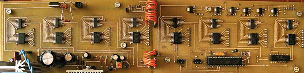
Note.0 - bit programmed, 1 - bit not programmed. The boards have eight (one for each display character) nodes A1-A8, which, under the control of the microcontroller, form the signals supplied to the combined cathodes of each row of LEDs of the matrix character. All these nodes are the same and are assembled according to the scheme shown in Fig. 3. Each has an MC74HC595AD chip that converts the serial code output by the microcontroller to parallel, and a set of open-collector current amplifiers based on composite transistors (ULN2803ADW chip). To each of the X1 connectors of the nodes A1-A8, the cathodes of the rows of LEDs of the corresponding familiarity are connected.
The microcontroller program alternately selects nodes A1-A8 to load codes into them, outputting a code from O to 0 (one less than the familiarity number) to the outputs PC2-PC7 of the microcontroller, and a signal to the output PC3 that allows the operation of the decoder DD2 (see Fig. 1). As a result, a low logic level is set at the decoder output corresponding to the code, which allows the DD1 chip connected to it (Fig. 3) to receive the serial code generated by the program at the PB3 output of the microcontroller. The signals generated at the outputs PD3-PD7 and amplified transistors VT2-VT6 alternately supply voltage to each of the five circuits that combine the anodes of the matrix LED columns. Speakers with the same number of eight characters are connected in parallel and turn on at the same time, which makes the display flickering less noticeable. Transistor VT1, controlled by a signal from the output PB0 of the microcontroller, allows you to turn off all the display LEDs at the same time. To power the display module, X8 is supplied with 9 V, 50 Hz. It can be obtained from any suitable step-down transformer. The author used a transformer TP-132-3 with a voltage on the secondary winding of 9 V at a load current of 0,5 A. The alternating voltage rectifies the VD2 diode bridge. The integrated stabilizer DA1 provides 5 V to the module's microcircuits. A stabilizer with an adjustable output voltage is built on a VT8 field-effect transistor and a DA2 parallel stabilizer. The circuit described by I. Nechaev in the article "A stabilizer with a small minimum voltage drop" was used. The voltage U set using the tuning resistor R17bright through transistors VT1-VT6 enters the anodes of the LEDs and determines the brightness of their glow. Additionally, the field-effect transistor VT7 controls the brightness. Its gate is energized from a variable resistor R11, fixed resistors R12, R13 and a voltage divider photoresistor R16. The resistance of the photoresistor decreases as the illumination of the place where the display is installed increases. As a result, the gate voltage of the transistor VT7 grows and it opens, which reduces the voltage Ubright and the brightness of the display LEDs. Variable resistor R11 set the optimal limits for automatic brightness changes. By removing jumper S1, automatic brightness control can be disabled. The LED matrix is located on two identical boards assembled according to the one shown in fig. 4 scheme. Connector X1 of the first LED board is connected to connector X5 of the board, the diagram of which is shown in fig. 1, and connectors X2-X5 with connectors X1 of nodes A1-A4 on the same board. Similarly, connect the second LED board to the one whose circuit is shown in fig. 2 using connector X11 and connectors Xl of nodes A5-A8.
Instead of discrete LEDs, to build a display, you can use ready-made LED sign-synthesizing matrices with an organization of 5x8 or 5x7 elements with anodes connected to the matrix columns. Please note that 5x7 matrices will not fully display all Russian letters. All printed circuit boards of the module are double-sided made of foil fiberglass with a thickness of 1,5 mm. A drawing of printed circuit conductors of the board on which the microcontroller and nodes A1-A4 are located is shown in fig. 5, and the location of parts on it - in Fig. 6.
The board with nodes A5-A8 is made according to the drawing shown in fig. 7, and the parts on it are arranged according to Fig. 8. On both boards, the item designations of parts related to nodes A1-A8 (including connectors) are provided with prefixes that match the node number, for example, 8DD1. Connectors X5, X11 and 1X1-8X1 are located on the sides of the boards opposite to where the rest of the parts are installed. This is done for the convenience of their direct docking with the connectors located on the LED matrix boards. A drawing of these boards (two of them are identical) is shown in fig. 9. The connectors on them are installed on the side opposite the LEDs. All boards use single row PBS (female) and PLS (male) connectors.
The exception is the two-row X1, X2 (PLD-6) and X10 (PBD-4) on the control boards. The character codes received from the source of information, the DD1 microcontroller program stores in RAM, and then analyzes and searches in the character generator table for the codes corresponding to the image of the desired character for display. A fragment of the character generator, consisting of ten blocks of 16 characters each, is given in Table. 2. Each character is described by five (according to the number of matrix columns) eight-bit (according to the number of matrix rows) binary codes. Units in these codes correspond to LEDs on, zeros to off. Table 2
The program rewrites the display codes of the character in the RAM cells, where they are temporarily stored before being displayed. The SPI hardware module of the microcontroller pushes these codes one by one into the serial registers of the 74HC595 microcircuits of the nodes A1-A8 for which they are intended. From here they are transferred to their storage registers by the signals generated at the PB2 output of the microcontroller. The total number of LED columns in an eight-digit display is 5x8=40. It is necessary to update information on it with a frequency of at least 100 Hz, otherwise flickering is possible. Thus, no more than 1/100/40 = 0,00025 s can be spent on writing information in one column - this is 4000 periods of the microcontroller clock frequency equal to 16 MHz. Program interrupt requests with approximately this period are generated by an eight-bit timer of the microcontroller with a prescaler of the clock frequency by 64. The timer recalculation factor is set to 62. The actual information update rate turned out to be 16000000/64/62/40=100,8 Hz. Whenever the displayed information needs to be changed, its source must send a packet of address and ten information bytes to the module via the TWI interface. The address byte must contain the address of the module with a zero (write flag) in the least significant bit. The first eight information bytes contain character codes that must be displayed in order from left to right. The upper four bits of the ninth byte must contain a number that is 7 units greater than the number of the flashing familiarity on the display (numbers are counted from 1 to 8 from left to right). When this byte is set to zero, flashing is disabled. The flashing period specifies the number in the tenth byte, each unit corresponds to 50 ms. The display module acknowledges to the source that it has received the correct address followed by nine data bytes. Reception of the tenth information byte is not acknowledged, which indicates the completion of the packet reception. After that, the module is again ready to receive the next packet. Before it is received, the previously received information is displayed on the display. Handling of reception errors in the microcontroller program is not performed. If a character code is received that is not in the character generator, a question mark in a rectangular frame will be displayed on the corresponding familiarity. There is no command to clear the display. Instead, an information packet with eight space characters ($20) should be sent. To prevent the display module from freezing, a watchdog timer is activated in its microcontroller. If the display control subroutine has never been called within 32 ms, the microcontroller is forced to reset and the program starts anew, as when the power is turned on. The appearance of the display module without a housing on the side of the LEDs is shown in fig. 10, and from the side of the installation of microcircuits - in fig. 11. Before turning on the assembled structure for the first time, it is necessary to set the minimum voltage value Ubright. The automatic brightness control unit is adjusted depending on the operating conditions of the display.
The module housing is from a Philips video player. The SDA and SCL lines are connected to the module via a two-way, two-position switch. In one position, information comes from any external source through a four-pin connector installed on the module case. In the second - from the electronic clock located in the same case, assembled according to the scheme shown in fig. 12.
The clock is built on an ATmega8535-16PU (DD1) microcontroller and a DS1307 (DD2) microcircuit - a real-time clock with an I interface2C. To communicate with the DD2 microcontroller, the DD1 microcontroller uses the same two-wire bus through which it transmits information to the display module. But the addresses of the chip ($D0) and the module ($A0) on the bus are different, which gives the watch microcontroller the ability to distinguish between them. Care must be taken that the addresses do not match when connecting the display module to other sources of information. The codes from the MasterDevice.hex file are entered into the FLASH memory of the watch microcontroller, and the configuration is programmed according to Table. 3. As in Table. 1, bit states that differ from those set by the manufacturer are highlighted in color. Table 3
Note. 0 - bit programmed, 1 - bit not programmed. The watch has seven control buttons. Their purpose: SB1 - setting the microcontroller to its original state, restarting the program; SB2 - switch to the time and date setting mode. The display briefly shows "Time". Then the name of the register, the contents of which are to be changed, and the value written in it are displayed; SB3 - transition from the current time display mode to the date display mode. In the time and date setting mode - the transition to the register with a lower address, which is shown on the display; SB4 - transition from the time and date setting mode to the current time display mode. Pressing this button starts the internal clock generator, counting seconds starts from zero. The display briefly shows "Done"; SB5 - writing a new value to the register, the display briefly shows the inscription "Write"; SB6 - increase the value for writing to the selected register, the recording itself occurs when you press the SB5 button; SB7 - transition from the date display mode to the current time display mode. In the time and date setting mode - decreasing the value for writing to the selected register, the recording itself occurs when the SB5 button is pressed. Programs for microcontrollers of the display module and clock can be downloaded from ftp://ftp.radio.ru/pub/2014/06/disp.zip. Author: N. Salimov
Traffic noise delays the growth of chicks
06.05.2024 Wireless speaker Samsung Music Frame HW-LS60D
06.05.2024 A New Way to Control and Manipulate Optical Signals
05.05.2024
▪ Insects are disappearing in the world ▪ Accelerator KFA2 GeForce GTX 960 EXOC White Edition ▪ Laser turrets for combat aircraft ▪ Adults evaluate children according to words
▪ section of the site Winged words, phraseological units. Selection of articles ▪ Robinson article. Popular expression ▪ article How does an octopus move? Detailed answer ▪ article Operator of impregnation of facing materials. Standard instruction on labor protection ▪ article T-contour. Encyclopedia of radio electronics and electrical engineering
Home page | Library | Articles | Website map | Site Reviews
www.diagram.com.ua | ||||||||||||||||||||||||||||||||||||||||||||||||||||||||||||||||||||||||||||||||||||||||||||||||||||


 Leave your comment on this article: