|
|


 Arabic
 Bengali
 Chinese
 English
 French
 German
 Hebrew
 Hindi
Hindi Italian
 Japanese
 Korean
 Malay
Malay Polish
 Portuguese
 Spanish
 Turkish
 Ukrainian
 Vietnamese
|
ENCYCLOPEDIA OF RADIO ELECTRONICS AND ELECTRICAL ENGINEERING Stabilization Uout capacitor rectifier. Encyclopedia of radio electronics and electrical engineering
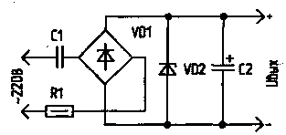
Encyclopedia of radio electronics and electrical engineering / Surge Protectors Judging by the latest publications [1...5], the interest of radio amateurs in low-power transformerless rectifiers with a quenching capacitor is not weakening. Indeed, with load powers in fractions and units of watts, they are more efficient than devices with a mains transformer or with a high-frequency converter. The disadvantage of the published designs of capacitor rectifiers is the sharp dependence of their output voltage on the presence or disconnection of the load and its magnitude. This dependence is usually eliminated by including a zener diode at the rectifier output, which is both a voltage stabilizer and an undesirable load ballast, since. consumes a current commensurate with the load current. Significant power is uselessly dissipated on it, and it has to be placed on a radiator. In [2], it required a radiator with an area of 25 cm2. The radiator increases the dimensions and weight of the rectifier, which is the second disadvantage. In [4], the author partially solved the first problem by using not one, but two network capacitors in the input circuit, connected as a capacitor divider. This led to an increase in the capacitance of the quenching capacitors and, accordingly, in dimensions and weight. In addition, the proportion of reactive current in the network has increased, which is also undesirable. I offer a transformerless capacitor rectifier with auto-stabilization of the output voltage in all possible operating modes (from idle to rated load), devoid of the listed disadvantages. This was achieved due to a fundamental change in the principle of generating the output voltage - not due to the voltage drop from the current pulses of the rectified half-waves of the mains voltage across the zener diode resistance, as in the described devices (Fig. 1), but due to a change in the time of connecting the diode bridge to the storage capacitor C2 ( Fig.2).
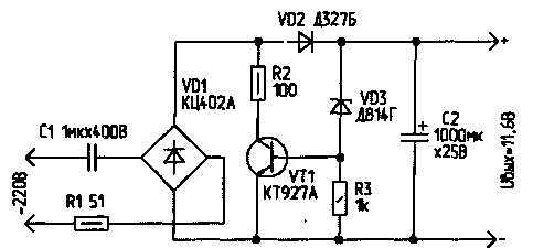
In the devices described, this time is constant and equal to the full period of the mains voltage. If, however, the output of the bridge is shorted with the key K for a part of the duration of the half-cycle of the network, and in the remaining part of the half-cycle, the key K is opened, and at this time the output current of the bridge charges the capacitor C2, then the voltage on it will depend on the share of this remaining part in relation to the entire half-cycle of the network . And if, as with PWM, you automatically change the time of the open state of the key depending on the voltage at C2, you can get auto-stabilization of the output voltage of the capacitor rectifier. The diagram of a stabilized capacitor rectifier is shown in Fig. 3. In parallel with the output of the diode bridge, the transistor VT1 is connected, operating in the key mode (key K in Fig. 2).
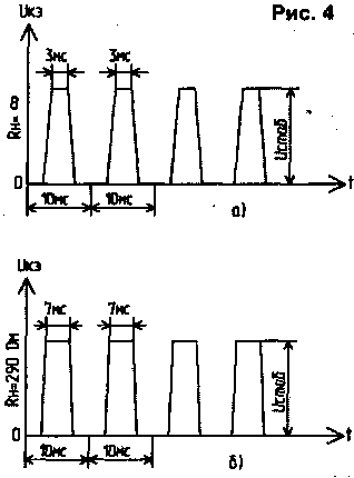
The base of the key transistor VT1 is connected through a threshold element (zener diode VD3) to a storage capacitor C2, separated by a direct current from the output of the bridge by a diode VD2 to prevent rapid discharge when VT1 is open. As long as the voltage on C2 is less than the stabilization voltage VD3, the rectifier works in a known way. When the voltage on C2 increases and VD3 opens, the transistor VT1 also opens and shunts the output of the rectifier bridge. As a result, the voltage at the output of the bridge abruptly decreases to almost zero, which leads to a decrease in the voltage on C2 and the subsequent turning off of the zener diode and the switching transistor. Further, the voltage across the capacitor C2 increases again until the zener diode and transistor are turned on, etc. These processes provide automatic stabilization of the output voltage. In the idle mode of the rectifier, the key transistor VT1 is open for most of the half-cycle of the mains voltage, and narrow current pulses with a long pause arrive at the storage capacitor C2 (Fig. 4a). When the load is connected, the duration of the open state of the transistor decreases (Fig. 4b). This leads to an increase in the duration of the current pulse coming through VD2 to C2, and an increase in the voltage across it, i.e. to maintain the output voltage at the same level. The process of auto-stabilization of the output voltage is very similar to the operation of a switching voltage regulator with pulse-width regulation. Only in the proposed device, the pulse repetition rate is equal to the voltage ripple frequency at C2 (in the circuit in Fig. 3, this frequency is 100 Hz).
The key transistor VT1 to reduce losses should be with a high gain, for example, composite KT972A, KT829A, KT827A, etc. The stabilized rectifier, assembled according to the scheme of Fig. 3, provides the output voltage: - at idle - 11,68 V; - at a load of 290 Ohm - 11,6V- Such a small difference in output voltages (only 0,08 V) confirms the good stabilization of the output voltage and the correct choice of the capacitance value of the quenching capacitor C1 for this load. With a decrease in its capacitance to 0,5 μF, this difference reaches 0,16 V. The ripple voltage at a load of 290 ohms does not exceed 40 mV. This value is determined by the capacitance of the smoothing capacitor C2 and the sensitivity of the base circuit VT1. You can increase the output voltage of the rectifier by using a higher voltage zener diode or two low voltage ones connected in series. With two zener diodes D814V and D814D and a capacitance of capacitor C1 of 2 μF, the output voltage at a load with a resistance of 250 ohms can be 23 ... 24 V. The examples given show how to experimentally select the elements of a transformerless capacitor rectifier for the required stabilized voltage at a given load. According to the proposed method, it is possible to stabilize the output voltage of a half-wave diode-capacitor rectifier, made, for example, according to the scheme of Fig.5. For a rectifier with a positive output voltage, a KT1A or KT972A npn transistor is connected in parallel with the VD829 diode, controlled from the rectifier output through the VD3 zener diode.
When the capacitor C2 reaches a voltage corresponding to the moment the zener diode opens, the transistor VT1 also opens. As a result, the amplitude of the positive half-wave of the voltage supplied to C2 through the VD2 diode decreases almost to zero. When the voltage on C2 decreases, the transistor VT1, thanks to the zener diode, closes, which leads to an increase in the output voltage. The process is accompanied by pulse-width regulation of the pulse duration at the input VD2, similar to how it happens in the rectifier according to the circuit in Fig.3. Consequently, the voltage across capacitor C2 remains stable both at idle and under load. In a rectifier with a negative output voltage, parallel to the VD1 diode, you need to turn on the p-n-p transistor KT973A or KT825A. The output stabilized voltage at a load with a resistance of 470 ohms is about 11V, the ripple voltage is 0,3 ... 0,4 V. In both proposed versions of the transformerless rectifier, the zener diode operates in a pulsed mode at a current of a few milliamps, which is in no way related to the load current of the rectifier, with a spread in the capacitance of the quenching capacitor and fluctuations in the mains voltage. Therefore, the losses in it are significantly reduced, and it does not require heat removal. The key transistor also does not require a radiator. Resistors R1, R2 in Fig. 3 and 5 limit the input current during transients at the moment the device is connected to the network. Due to the inevitable "bounce" of the contacts of the mains plug and socket, the switching process is accompanied by a series of short circuits and circuit breaks. With one of these short circuits, the quenching capacitor C1 can charge up to the full amplitude value of the mains voltage, i.e. up to about 300 V. After a break and subsequent short circuit due to "bounce", this and the mains voltage can add up to a total of about 600 V. This is the worst case that must be taken into account to ensure reliable operation of the device. Specific example: the maximum collector current of the KT972A transistor is 4 A, so the total resistance of the limiting resistors should be 600V/4A=150 Ohm. In order to reduce losses, the resistance of the resistor R1 can be selected as 51 ohms, and the resistor R2 - 100 ohms. Their dissipation power is not less than 0,5 W. The allowable collector current of the KT827A transistor is 20 A, so resistor R2 is optional for it. Literature 1. Dorofeev M. Transformerless with a quenching capacitor. - Radio, 1995, N1, S. 41,42; #2, p.36,37. Author: N.Tsesaruk, Tula; Publication: N. Bolshakov, rf.atnn.ru
Artificial leather for touch emulation
15.04.2024 Petgugu Global cat litter
15.04.2024 The attractiveness of caring men
14.04.2024
▪ Prosthesis that senses touch ▪ CRT TV with built-in DVD recorder from PANASONIC ▪ Cloning of ancient animals is discussed by Russian scientists ▪ Helium hard drives are expected to grow in popularity
▪ section of the site Security and safety. Article selection ▪ article Simple hammock. Tips for the home master ▪ article Can a dolphin talk? Detailed answer ▪ article Giardiasis. Health care ▪ article Rolling cigarette. Focus Secret
Home page | Library | Articles | Website map | Site Reviews
www.diagram.com.ua |


 Leave your comment on this article: