|
|


 Arabic
 Bengali
 Chinese
 English
 French
 German
 Hebrew
 Hindi
Hindi Italian
 Japanese
 Korean
 Malay
Malay Polish
 Portuguese
 Spanish
 Turkish
 Ukrainian
 Vietnamese
|
ENCYCLOPEDIA OF RADIO ELECTRONICS AND ELECTRICAL ENGINEERING USB voltage recorder with oscilloscope, spectrum analyzer and frequency response meter functions. Encyclopedia of radio electronics and electrical engineering
Encyclopedia of radio electronics and electrical engineering / Measuring technology The hardware part of this recorder is an ADC equipped with a high-speed communication channel with a computer via the USB bus, implemented using a programmable logic chip (FPGA). And the computer program developed by the author allows not only to record the digitized signal to a file, but also to display its oscillogram, spectrum, and even measure the amplitude-frequency response (AFC) of a filter or other linear device, to the input of which a test signal is applied from the generator built into the recorder. In the recorder under consideration, the samples of the signal under study, which the ADC takes at a frequency of 960 kHz, are fed to the input of the FPGA, which converts the parallel code of the ADC to serial. In each group of five eight-bit bytes transmitted further to the UART-USB converter, the FPGA places four ten-bit ADC codes. Further, the information is transmitted via USB to a computer for processing and storage. The communication protocol with a computer and other functions in the recorder are implemented using a microcontroller. The FPGA and the microcontroller are programmed through the same UART-USB converter that is used to transfer information. To work with the recorder, a program was developed in the LabVIEW environment that implements the reception of information, its display and storage. In addition, it implements an algorithm for removing the frequency response of an external circuit connected to the recorder at frequencies from 0,1 Hz to 480 kHz. A distinctive feature of this algorithm is that to estimate the amplitude-frequency characteristic of the circuit under study, the harmonics of the repetition frequency of rectangular pulses generated by the recorder's microcontroller are used. The task set to develop a device for continuous transmission to a computer in real time of readings of the instantaneous voltage value in the range from 15 to +15 V with a sampling frequency of 960 kHz and a resolution of ten binary digits, in principle, could be solved without an FPGA using an ADC and a microcontroller with built-in USB port operating as a virtual COM port. However, the speed of information transfer in this case would not be high enough. When used together with the ADC and the microcontroller, the FT2232H UART-USB interface converter microcircuit, which provides information transfer at a speed of 12 Mbps, there is a problem of finding a microcontroller whose UART is capable of operating at such a speed. As a result, a method was chosen that differs from the previous one by using an FPGA that reads the information generated by the ADC in parallel code and converts it into a serial format characteristic of UART. The device uses a ten-bit ADC10030 ADC with parallel output and a maximum sampling rate of 30 MHz. The results of his work are received and processed by the EPM3064ALC44-10N FPGA, which contains 64 programmable logical macro cells and 44 I / O lines. Each input signal sample generated by the ADC is a ten-bit binary code, and the FT2232H UART-USB converter receives information in eight-bit bytes. For this reason, the FPGA implements a device that packs every four samples into five bytes. Next, it supplies each byte with start and stop bits and transfers them in serial code at 12 Mbaud to the FT2232H chip for transfer to a computer via USB. The diagram of the recorder is shown in fig. 1. It is powered by a constant voltage of 7 ... 9 V supplied from the XP3 connector to the integrated stabilizer DA6 7805, and from it, with a removable jumper S4 in position 1-2, to a voltage regulator of 3,3 V LM1117-3.3 (DA7). For the convenience of working with the device during debugging, it is possible to power it from the USB port. To do this, the removable jumper S4 should be rearranged to position 2-3. However, during normal operation, such power supply is unacceptable, since the voltage taken from the USB port often differs noticeably from 5 V, which leads to a change in the conversion scale of the signal under study in the ADC.
The 24 MHz clock generator for ADC and FPGA is built on the elements of the DD2 74HC04D chip and stabilized by the ZQ2 quartz resonator. To implement the protocol for communication with a computer, the formation of discrete signals and the generation of rectangular pulses, a DD1 ATMega8A microcontroller was introduced into the recorder, operating at a clock frequency of 16 MHz, specified by a ZQ1 quartz resonator. The exchange of information between the computer and the microcontroller also takes place using the FT2232H (DD4) chip, but via a different channel. To communicate with the FPGA and with the microcontroller, two virtual COM ports must be organized in the operating system of the computer working with the recorder. The signal under study is fed through the XP1 connector to the input of the DA2 AD825ARZ op-amp stage, which is a 15-fold inverting signal attenuator. The zero level at the output of the op-amp DA2 can be biased using the trimmer resistor R1. Thus, the signal under study is brought to the allowable range of the ADC input voltage change. Op-amp DA2 is powered by a voltage of +/-15 V, which forms from +5 V a DC unipolar voltage converter into a bipolar AM1D-0515DH30Z (U1). Resistors R19 and R20 are the minimum converter load necessary for its proper operation. By rearranging the removable jumpers S1 and S2 from position 2-3 to position 1-2, you can switch to powering the DA2 microcircuit with an external voltage of +/- 15 V applied to the XP4 connector. If desired, you can power external devices with a current consumption of not more than 1 mA from the converter U35. Reference voltages for ADC DA5 are formed by op amps DA3.1 and DA3.2 according to the scheme recommended in the description of the ADC. The parallel code from the ADC outputs goes to the DD3 FPGA, where it is converted into a serial UART code. Then it goes to the DD4 FT2232H chip. The XP2 connector is designed to control external devices with 3,3 V logic level signals over eight channels, in addition, a 3,3 V DC voltage and a common wire are connected to this connector to power external devices. Connectors XP5 and XP6 are designed for programming devices connected to them with a supply voltage of 3,3 V. Voltages of 7 V, 3,3 V and a common wire for powering external devices, a pulse signal with a frequency of 5 MHz (clock frequency of the ADC and FPGA) are output to the XP24 connector. Pin 4 of this connector is connected to pin 14 of the DD3 FPGA, which is not used in the described version of the device. LEDs are connected to the XP8 connector, signaling the operating mode of the converter: HL1 - presence of supply voltage; HL2 - transfer of information from the microcontroller to the computer; HL3 - transfer of information from a computer to a microcontroller; HL4 - transfer of information from the FPGA to the computer; HL5 - transfer of information from the computer to the FPGA; HL6 - the generator of rectangular pulses is included; HL7 - transfer of information from the FPGA is allowed by the microcontroller; HL8 - FPGA transmits information. A drawing of the PCB conductors is shown in fig. 2 (side 1) and fig. 3 (side 2). The location of the elements on these sides of the board - respectively in fig. 4 and fig. 5. The board provides space for elements not shown in the diagram, from which you can assemble a U-shaped input attenuator or filter between the XP1 connector and the R4 resistor and an L-shaped filter between the DA2 output of the op-amp and the DA5 ADC input. To pass the signal in the absence of an attenuator and a filter, jumpers for surface mounting are installed instead of their serial elements. Two more jumpers replace the resistors connected in series with resistors R5 and R8 if it is necessary to accurately select the ADC reference voltage.
For the DD3 FPGA in the PLCC-44 package, a panel must be installed on the board. The integral stabilizer DA6 is mounted on a ribbed heat sink measuring 22x20x15 mm. The recorder is assembled in a Gainta G715 case; its appearance is shown in fig. 6. LEDs are fixed on the front panel and holes for XP1, XP2, XP4, XP7 connectors are made. From the rear panel there is access to the switch block SA1, connectors XS1, XP5, XP6.
The structure of the device implemented in the FPGA is described in the VDHL language. Translation and debugging were performed in the Quartus 11 Version 10.1 development environment. Input signals: clk - clock signal; P - array of signals coming from the microcontroller; ADC_data - array of signals coming from ADC; rx - signal coming from FT2232H. Output signals: P1 - signal intended for the microcontroller; tx - signal intended for FT2232H; PHL - signal that controls the LED HL8; PPD - ADC power off signal; POE - ADC output enable signal; POUT - the signal output to the XP7 connector. Variables: count - counter of the number of bytes transferred; start_bit - indication of the start of byte transfer; stop_bit - sign of completion of data transfer; ADC_data_buf - ADC information storage buffer; rx_bit - a sign of the beginning of receiving information. Upon the transition of the clock signal from a low to a high level, the reception of the starting discharge is checked (Table 1). Then, if the transmission is in progress, the contents of the counter of transmitted bytes are increased by one (Table 2). When the content of the counter reaches the value 100, it occurs according to the table. 3, it is set to zero, and a check is made for the presence of a transmission completion command (P(6)=0). Table 1
Table 2
Table 3
Upon the transition of the clock signal from high to low, before the start of transmission, buffering of information from the ADC is performed (Table 4) in order to prevent its change during transmission. Table 4
The rest of the steps are to check the permission or prohibition of the transfer of information from the microcontroller. In the enabled state, the HL8 LED turns on and the sign of the completion of the transfer is removed if the request byte was received (Table 5). The transfer of the start and stop bits is carried out according to Table. 6, and information from the ADC buffer - Table. 7 (each bit is transmitted in two count cycles). Table 5
Table 6
Table 7
The program for the microcontroller is written in C language in the ImageCraft development environment. After powering up the device, it initializes the microcontroller peripherals, then enters the main loop, with the microcontroller UART in the receive standby mode. Upon receipt of a byte, an interrupt handler is launched (Table 8). This byte is written to the rx_arr array at the rx_count index (if the first byte of the packet was received, then rx_count=0), after which rx_count is incremented by one. This is followed by a restart of timer 0, the expiration of which serves as a sign of the end of the packet. Table 8
If the next byte is not received within the specified time, then an interrupt occurs at the request of timer 0. In the handler of this interrupt (Table 9), the timer is stopped and the receive end flag f_rx is set. Table 9
When an information packet is received (f_rx= 1), the main loop starts parsing it, executing the commands contained in it, and generating responses. First, the header and end of the packet are checked, then the command code. After a successful check, the execution of the command contained in the package begins. If an error is detected, a negative receipt is generated. The following commands are implemented in the program: - "Test" - is used to check the connection; - "Set IO states" - sets the specified logical levels on the microcontroller pins connected to the XP2 connector. Connector pin 2 (IO1 circuit) corresponds to the LSB of the command data byte, and pin 9 (IO8 circuit) corresponds to the MSB; - "Set FPGA-related IO states" - sets the specified logical levels at the microcontroller outputs PD4-PD7, PB1, PC2, PC3, associated with the FPGA. The outputs are listed in the order of their respective command data byte bits from one to seven. The value of the least significant (zero) byte of the byte can be arbitrary, since the state of the PD3 output is not available for change by this command. It is used to receive an interrupt request from the FPGA; - "Start the generator of rectangular pulses (with a period that is a multiple of 2 s)" - launches the specified generator of rectangular pulses (the duty cycle of all pulses generated by the recorder is equal to two). The command data byte must contain the value of the pulse repetition period, which can be in the interval of 2-2 s in steps of 254 s. Pulses are generated at the output of the microcontroller PB3 by software switching its state in the interrupt handler from timer 1. They are output to pin 5 of the XP2 connector; - "Start the generator of rectangular pulses (with a period that is a multiple of 2 s) after starting the ADC" - differs from the previous command in that it starts the generator synchronously with the start of information transfer from the FPGA to the computer; - "Start square-wave generator" - starts the square-wave generator with frequency from 30 Hz to 8 MHz. The four bytes of data must contain the frequency value in hertz. The generator is turned off by setting the frequency to zero. Since the repetition period of the generated pulses is always a multiple of the duration of the microcontroller machine cycle, the actual frequency of their repetition may differ from the specified one. Its exact value (with a resolution of 1 Hz) is contained in the response to the command. The pulses are output to pin 5 of the XP2 connector, connected to the PB3 output of the microcontroller. To start the transfer of information from the FPGA, it is necessary to enable it by setting a high logic level at the input 16 of the FPGA, and then transfer one byte through the COM port to the FPGA. The permission was introduced for the convenience of terminating the transmission by setting the input 16 of the FPGA to a logical zero. Since the transfer is allowed by the microcontroller, in order to synchronize the start of transmission from the FPGA with the start of receiving information by the computer, the latter must send an arbitrary request byte to the microcontroller. The microcontroller communicates with the computer at a rate of 1 Mbaud with eight bits without parity and one stop bit. To exchange information via USB through the FT2232H chip of the recorder in the operating system of the computer, you need to install the drivers that can be found on the Internet page [1]. Loading programs into the FPGA and the microcontroller. FPGA programming is performed according to the method described in [2]. Before starting it, it is necessary to set the DIP switches SA1 - SA3 to the positions shown in fig. 7a. The microcontroller was programmed using the AVRDude program and the SinaProg graphical shell, downloaded from the links on the Internet page [3]. SinaProg requires the LabView RunTime Library [4] to be installed on the computer.
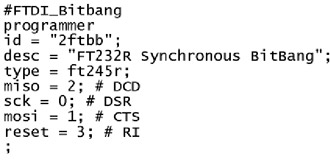
In the avrdude.conf file, it is necessary to reassign the pins of the 2ftbb programmer, supplementing the text of the file with the section shown in Table. 10. Table 10
The appendix to the article contains the programs AVRDude and SinaProg, in which all the necessary parameters are already set. Starting programming the microcontroller, you should set the switches SA1-SA3 of the registrar to the positions shown in fig. 7b, then connect the XS1 connector of the recorder to the USB port of the computer and run the SinaProg program. In the "Programmer" field of its window, set the parameters 2ftbb, FTDI, 9600. Then, in turn, press the on-screen buttons "<" and "Search", after which a text similar to that shown in Table 11 should appear in the message window. eleven . Using the menu called by pressing the "Advanced" screen button of the "Fuses" field, set the microcontroller configuration: high - 0xC9, low - 0xFF. In the "Hex file" field, specify the name of the HEX file with the microcontroller program codes and click the Program button in the Flash field. Upon successful completion of programming, a text ending with the lines shown in Table 12 should appear in the message field. XNUMX. Table 11
Table 12
If the recorder is used for programming devices connected to the XP6 or XP7 connector, the SA1-SA3 switches must be set to the positions shown in fig. 7, c. The positions of the switches during normal operation of the recorder are shown in fig. 7, g. Computer program USB-960 was developed in the LabVIEW 2011 environment. If this environment is not available on the computer, then packages [5] and [6] will need to be installed. The program contains eleven virtual sub-devices (VP): - ACPPLISUC_IOUC sets the states of the microcontroller output ports output to an external connector; - ACPPLISUC_FREQ starts the generator with subsequent measurement of the generated frequency; - ACPPLISUC_TEST checks the connection with the microcontroller; - ACPPLISUC_AFR_H measures the frequency response of the external circuit at five frequency values (not lower than 30,5 Hz); - ACPPLISUC_AFR_L measures the frequency response of the external circuit at a frequency from fractions to tens of hertz; - ACPPLISUC_GEN2S starts a rectangular pulse generator with a repetition period that is a multiple of 2 s; - ACPPLISUC_UNPACKDATA converts information received from the registrar into an array of ADC code values; - ACPPLISUC_ADCDATA reads information received from the registrar during the specified time; - ACPPLISUC_IOPLIS sets the states of the microcontroller output ports associated with the FPGA; - ACPPLISUC_GEN starts a rectangular pulse generator with a repetition rate of 30,5 Hz and higher; - ACPPLISUC_GEN2Ss starts the generator of rectangular pulses with a period that is a multiple of two seconds, synchronously with the start of reading information from the registrar; - ACPPLISUC_COM receives and transmits information through the virtual COM port associated with the microcontroller. The main program runs in an infinite while loop, inside of which there is a case structure, its current page is determined by the selection of a tab in the main program window. Signal Recording Tab shown in fig. 8. Pressing the "START" button starts receiving readings of the signal under study for the time specified in the "Measurement time, s" field. To do this, the transfer of information from the FPGA is allowed - the value 128 is written to the ACPPLI-SUC_IOPLIS VI. The actual reading is performed using the ACPPLISUC_ADCDATA VI, whose parameter is the measurement time. This VI requests information by passing a null byte and reads it for the specified time. After it expires, the transfer is disabled by writing a zero value to the ACPPLISUCJOPLIS VI.
If the "Write to file" button was previously pressed, then the signal under study is saved in a binary file, the name of which is specified in the "File to save the signal" field. By default, saving is done to the root folder of drive C, which may require the computer's operating system to run the program with administrator rights. The start of the generator of rectangular pulses is carried out in the fields "Generator start" and "Generator start with a period that is a multiple of 2 seconds". Upon completion of reception, the oscillogram of the received signal is displayed in the "Signal" field, and its spectrum is displayed in the "Amplitude spectrum" field. In the "RMS, V" and "Average value, V" fields, the rms and average values of the signal will be displayed, respectively. Oscilloscope tab shown in fig. 9. Pressing the on-screen button "START" starts the while loop, in which repeatedly (until pressing the "STOP" button) information is received from the registrar according to the algorithm similar to that described above. To avoid signal clipping during synchronization and manual offset, the actual recording duration is twice the specified one. Upon its completion, the signal searches for the moments of crossing the specified threshold (set using the "Threshold, B" controller), from which an array is formed. Then, in this array, the program finds an element located as close as possible to 1/3 of the signal duration. It will be used as the starting point of the waveform displayed on the screen.
Using the "Offset, %" slider, you can shift the waveform. The "Save current signal" and "Read" buttons save the currently displayed signal and read the previously saved signal. Tab "Removal of frequency response" shown in fig. 10. It is possible to determine the frequency response of a linear circuit [7] by simultaneously or sequentially exposing its input to harmonic signals of various frequencies, followed by measuring the amplitude of these signals at the output of the circuit. In the device under consideration for measuring the frequency response, instead of harmonic signals, rectangular pulses generated by the microcontroller are used. A signal in the form of rectangular pulses with a duty cycle of 2 is the sum of an infinite number of harmonic signals (harmonics), whose frequencies are an odd number of times higher than the pulse repetition rate. The amplitudes of its harmonics are approximately equal to 0,9 (first), 0,3 (third), 0,18 (fifth), 0,129 (seventh), 0,1 (ninth) pulse amplitudes. Knowing the ratio of harmonics (spectrum) of the signal at the input of the circuit under study and determining it at the output, it is possible to calculate the frequency response of this circuit at harmonic frequencies.
The registrar removes the frequency response using rectangular pulses with a duty cycle of 2 and a repetition rate of 0,1; 0,5; 30,5, 60,1, 120,2, 240, 480,8, 961,5, 1923, 3846, 7692,3, 15384,6, 31250 and 61538,5 Hz. Pressing one of the "START 0,1 Hz" or "START 0,5 Hz" screen buttons starts the ACPPLISUC_AFR_L VI with a period of 10 s and 2 s, respectively. This VI works like this: - using the VI ACPPLISUC_GEN2SS sends a command to start the generator of rectangular pulses with a given period; - receives information from the ADC during 1,5 pulse repetition periods; - Passes the received signal through a 2000 Hz digital low-pass filter to remove high-frequency components before signal decimation. If this is not done, the effect of aliasing will occur [8]; - thins the signal, discarding 47 out of every 48 of its samples, in order to simplify further calculations; - extracts from the signal a fragment with a duration of exactly one pulse repetition period; - calculates the amplitude spectrum of this fragment; - extracts from the obtained spectrum the components corresponding to the odd harmonics of the test signal, divides them into known amplitude values of the same harmonics of the original signal. The result is the frequency response of the circuit under study at harmonic frequencies. When the "START 30 Hz" screen button is pressed, the for loop is launched, in which the ACPPLISUC_AFR_H VI is executed, the input of which receives the pulse frequency and measurement time values. At the output of this VP, the frequency response values at five harmonics of the signal of a given frequency are obtained. As a result of the cycle, three arrays are formed: frequencies at which the frequency response was measured, signals used to calculate the frequency response, and frequency response values. Next, the array of frequency response values is sorted for further display of its graph on the screen. The ACPPLISUC_AFR_H VI works as follows: - using the VI ACPPLISUC_GEN sends a command to start the generator; - receives information from the ADC within a specified time; - calculates the amplitude spectrum of the recorded signal; - from the obtained spectrum extracts five components corresponding to the harmonics of the test signal, divides their values by the relative amplitudes of the harmonics of the signal applied to the input of the circuit under study. As a result, five readings of the frequency response are obtained. It should be noted that the duration of the analyzed signals must necessarily be exactly a multiple of the pulse repetition period, otherwise, when calculating the spectrum, its "spreading" [9] or "leakage" [7] will occur, and the analysis results will be distorted. Pressing the on-screen buttons "Save results" and "Read" writes the currently displayed frequency response to the disk file and reads the frequency response recorded earlier. To test the operation of the recorder in the frequency response reading mode, a node assembled on a prototyping board was connected to it according to the circuit shown in Fig. 11. These are R1C2 low-pass and R2C1 high-pass filters. Buffer followers on the op amp of the DA1 chip eliminate the effect on the frequency response of the filters of a relatively high output impedance of the generator output and a low (1,5 kOhm) input impedance of the recorder. The voltage +15 V and -15 V to power the DA1 microcircuit can be removed from the Xp4 connector of the recorder, if you connect each three pins on the board of the latter to each other, intended for jumpers S1 and S2 (not to be confused with jumpers S1 and S2 in Fig. 11, which are switched filters).
To compare the measured frequency response with those obtained by calculation, the program "Comparison_AFC_with_calculation" was created, which calculates the frequency response of a given RC circuit and plots it in the same coordinates with the measured one. The results are presented in fig. 12 (low pass filter) and fig. 13 (high pass filter). The calculated values are shown in red, the measured values are shown in white. Further, capacitors with a capacity of 1 μF were connected in parallel with C2 and C8 and the characteristics shown in Fig. 14 and fig. 15.
Calibration tab shown in fig. 16. When performing this operation, it is necessary to set the relationship between the voltage at the input of the recorder and the value of the code at the output of the ADC. Since this dependence is linear, it suffices to enter the coordinates of its two points. To do this, a constant voltage close to the maximum is applied to the input of the recorder. Its value is recorded in the "Umax, V" field. In the field "ADC-avg." the value of the ADC output code averaged by the program will be displayed. It can be entered into the "ADC-max" field manually or use the on-screen button "Write current ADC-average value as ADC-max".
Having applied a constant voltage close to the minimum to the input of the device, similarly enter the values in the fields "Umin, V" and "ADC-min". As already mentioned, the actual frequencies of the signals generated during the removal of the frequency response of the signals may differ slightly from the specified values, due to which it is impossible to know in advance the exact durations of the samples to be analyzed, which must be a multiple of an integer number of signal periods. The actual frequency values must first be measured and the sample durations calculated. These actions are performed in a case-structure called by the button "Define periods for reading frequency response", the results are saved in a text file. Calibration is performed as follows: - connect the input of the device to a common wire by connecting the contacts of the XP1 connector; - trimming resistor R1 set in the window "ADC-average." values from 511 to 513 (by clicking on the "Read" screen button to update); - connect a DC voltage source +1...13 V to the XP15 connector, enter the exact value of this voltage in the "Umax, V" field; - click on the "Read" screen button to digitize the signal and determine the average value of the ADC code, then click on the screen button "Write the current value of ADC-average as ADC-max"; - reverse the polarity of the voltage applied to the XP1 connector, enter its value in the "Umin, V" field, click on the "Read" screen buttons, and then "Write the current value of ADC-average as ADC-min"; - having disconnected the voltage source from connector XP1, connect pin 1 of this connector to pin 5 of connector XP2 and press the on-screen button "Determine logic level voltage (IL1)". This value is required to calculate the frequency response; - press the on-screen button "Define periods for taking frequency response" and wait for the end of measurements (the process takes more than two minutes). The measurement results are stored in a text file on the computer's hard drive. The name of this file and the path to it are contained in the "File with calibration coefficients" field; - by pressing the on-screen button "TEST" a test command is sent to the microcontroller, if the correct answer is received, the indicator "TEST OK" will be turned on. In the "IO" field, you can manually set the states of the microcontroller outputs output to the XP2 connector, and in the "IO-PLIS" field - those associated with the FPGA. In conclusion, it can be noted that if you build a recorder based on the Xilinx Spartan-3 FPGA with a MicroBlaze processor core, then there will be no need to use a microcontroller. PCB file in Sprint Layout 5.0 format and programs for FPGA, microcontroller and computer can be downloaded from ftp://ftp.radio.ru/pub/2014/11/usb-reg.zip. Literature
Author: V. Tchaikovsky
Artificial leather for touch emulation
15.04.2024 Petgugu Global cat litter
15.04.2024 The attractiveness of caring men
14.04.2024
▪ Molecular memory works at room temperature ▪ Meditation speeds up the brain ▪ Hot water instead of oil and gas ▪ Space Rider Orbital Laboratory ▪ Sensor for smart home Mi Human Sensor 2
▪ radio section of the website. Article selection ▪ article Gifts of Pomona and Flora. Popular expression ▪ How does a caterpillar turn into a butterfly? Detailed answer ▪ Grand Canyon article. Nature miracle ▪ article Fractional quantum Hall effect. Encyclopedia of radio electronics and electrical engineering
Home page | Library | Articles | Website map | Site Reviews
www.diagram.com.ua |


 Leave your comment on this article: