|
|


 Arabic
 Bengali
 Chinese
 English
 French
 German
 Hebrew
 Hindi
Hindi Italian
 Japanese
 Korean
 Malay
Malay Polish
 Portuguese
 Spanish
 Turkish
 Ukrainian
 Vietnamese
|
ENCYCLOPEDIA OF RADIO ELECTRONICS AND ELECTRICAL ENGINEERING Powerful pulse stabilized power supply. Encyclopedia of radio electronics and electrical engineering
Encyclopedia of radio electronics and electrical engineering / Power Supplies The article brought to the attention of readers describes a powerful switching source for powering various electronic equipment. It is assembled according to the scheme of a half-bridge inverter controlled by a TL494 SHI controller. The emergence of high-power high-voltage field-effect transistors was a prerequisite for the development of high-frequency network power supplies with pulse-width (PW) control [1,2, 3]. The main advantages of such sources over traditional linear ones are obtaining more power at the load with smaller dimensions and, accordingly, greater efficiency [XNUMX]. The scheme of the proposed switching power supply is shown in fig. 1. The basis of the device is a converter assembled according to a half-bridge circuit. The power supply has a complete galvanic isolation between the input high-voltage and output circuits. The control unit is assembled on the basis of the TL494 SHI controller.
Main technical specifications of the power supply
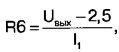
Transistor optocoupler U2 provides galvanic isolation in the negative voltage feedback circuit. The voltage drop across the resistor R7 is approximately 2,5 V. The resistance of this resistor is calculated by setting the current through the resistive divider R6R7. The resistance of the resistor R6 is calculated by the formula
where Uvyx - output voltage of the power supply; I1 - current through the resistive divider R6R7. The resistance of the resistor R9 determines the current through the emitting diode of the optocoupler U2.1, as well as the minimum operating current of the stabilizer DA1. With the selected current in this circuit I2 (the current value must be within the acceptable limits for the stabilizer DA1), the resistance of the resistor R9 is calculated by the formula
where UF is the voltage drop across the emitting diode of the optocoupler U2.1. The DA5 chip stabilizes the voltage of 8 V to power the divider, which consists of the U2.2 optocoupler phototransistor and the R17 resistor. The voltage from the middle point of the divider is fed to the non-inverting input of the first error signal amplifier of the DA6 SHI controller. The voltage for powering the control unit and drivers (DA7 chip) of field-effect transistors provides an auxiliary source on the network transformer T2 and analog voltage regulators DA2 and DA3. The current protection node is assembled on the DA4 comparator and the DD1.1 trigger. The function of the current sensor is performed by the resistor R5, included in the diagonal of the half-bridge. A triangular-shaped voltage is supplied to the non-inverting input of the comparator DA4 from the capacitor (C26) of the frequency-setting circuit of the clock generator of the SHI controller (Fig. 2). At the output of the comparator, clock pulses are generated, which are fed to the input C of the trigger DD1.1.
If the voltage drop across the resistor R5 reaches 1,1V, the emitting diodes turn on and the phototransistor of the optocoupler U1 opens. The input S trigger DD1.1 will go low. At the direct output of the trigger DD1.1 and, therefore, at the non-inverting input of the second error signal amplifier of the SHI controller DA6, a high level will be set. In this case, both transistors VT1 and VT2 will be closed. To control powerful switching field-effect transistors, a specialized microcircuit is used - a two-channel driver DA7. On fig. 3 shows the internal structure of one channel. Numbers of outputs of the second channel are indicated in brackets. Each channel contains an optocoupler and an amplifier with a high current output. Such microcircuits are widely used to control both asynchronous and DC motors. The driver parameters allow you to directly control the field-effect transistors with an insulated gate, switching current up to 50 A at a voltage not exceeding 1200 V. Main parameters of the HCPL315J chip
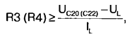
The resistance of resistors R3 and R4 in the gate circuits of switching transistors is calculated by the formula
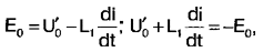
where UC2o (C22) is the driver supply voltage (voltage across capacitor C20 or C22); UL - driver output voltage; lL is the maximum peak output current. The half-bridge diagonal includes the primary winding of the transformer T1 and the inductor L2 (the inductance of the inductor may include the leakage inductance of the transformer) [4]. The transformer is made on the magnetic circuit E-E, size F-43515 from Magnetics Inc. The primary has 38 turns of #19AWG wire and the secondary has 5+5 turns of #12AWG wire. The L2 inductor is wound on an F-41808EC magnetic circuit from Magnetics Inc. The L2 inductor winding consists of 8 turns of #19AWG wire. The inductor L3 is made on a toroidal magnetic circuit MPP 55930A2 from Magnetics Inc. The L3 inductor winding contains 20 turns of #12AWG wire. The input filter inductor L1 is E3993 from Coilcraft, its inductance is 900 μH. When the transistor VT1 (or VT2) is turned on, a linearly increasing current begins to flow through the primary winding of the transformer T1 during the control pulse t1 (Fig. 4). When the transistor VT1 (or VT2) closes, due to the energy accumulated in the primary winding of the transformer and inductor L2, a linearly decreasing current continues to flow in the circuit during the time t2 in the same direction. It closes through the VD7 diode if the VT1 transistor is turned off (or through the VD6 diode if the VT2 transistor is turned off).
Without taking into account the active power losses in the primary circuit of the transformer, we write the equations for the time intervals t1 and t2:
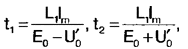
where E0 \u2d Upit / 0 - half the supply voltage; U'1 - output voltage of the source, reduced to the primary winding of the transformer; L1 is the total inductance of the primary winding of the transformer T2 and inductor LXNUMX. From here we obtain expressions for the time t1 and t2 (see Fig. 4):
where lm is the maximum current of the primary winding of the transformer. The time of current flow through the primary winding of the transformer in one direction tn = t1 + t2 can be expressed as follows:
If we accept that
then the current flow time is
From this equality, we obtain an equation for the external characteristic of the power source. For example, for the duty cycle of control pulses
should
whence
If we denote
then the equation of the external characteristic of the power supply has the form
The external characteristic of the power supply is shown in fig. 5. The output voltage of the source depends on the resistance of the resistor R17 - the lower the resistance, the lower the output voltage. The protection trip current is determined by the resistance of the sensor - resistor R5. Literature
Authors: R.Karov, S.Ivanov, Sofia, Bulgaria
Machine for thinning flowers in gardens
02.05.2024 Advanced Infrared Microscope
02.05.2024 Air trap for insects
01.05.2024
▪ The updated line of Wireless Plus from Seagate ▪ The robot performed before the British House of Lords
▪ section of the site Intercoms. Article selection ▪ Humpbacked Grave's article will fix it. The art of audio ▪ article Which writer got the stone that lay on Gogol's first grave? Detailed answer ▪ article Crusher. Job description ▪ article Digital phosphor oscilloscopes. Encyclopedia of radio electronics and electrical engineering ▪ article Broadband power amplifier. Encyclopedia of radio electronics and electrical engineering
Home page | Library | Articles | Website map | Site Reviews
www.diagram.com.ua |


 Leave your comment on this article: