|
|


 Arabic
 Bengali
 Chinese
 English
 French
 German
 Hebrew
 Hindi
Hindi Italian
 Japanese
 Korean
 Malay
Malay Polish
 Portuguese
 Spanish
 Turkish
 Ukrainian
 Vietnamese
|
ENCYCLOPEDIA OF RADIO ELECTRONICS AND ELECTRICAL ENGINEERING
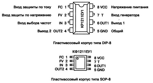
Electronic ballast powered by low-voltage sources. Electronic ballast on the KR1211EU1 chip. Encyclopedia of radio electronics and electrical engineering
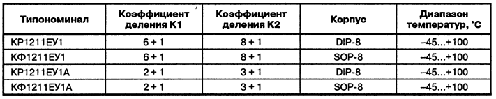
Encyclopedia of radio electronics and electrical engineering / Ballasts for fluorescent lamps This version of the power supply from a low-voltage source is an electronic ballast implemented on a specialized microcircuit KR1211EU1. Chip KR1211EU1 is a specialized controller for electronic ballasts (ballasts) for compact fluorescent lamps powered by an on-board DC network of 3-24 V. Produced using CMOS technology. In table. 3.12 shows the distinctive characteristics of microcircuits in different cases. The pinout of the cases and the assignment of the conclusions are shown in fig. 3.56.
Table 3.12. Differences of microcircuits with different markings
Maximum values of parameters and modes:
Electrical specifications:
Description of work. The block diagram of the 1211EU1/A microcircuit is shown in fig. 3.57.
Summary feature microcircuits KR (KF) 1211EU1 - the presence of two sufficiently powerful key control channels operating in antiphase with a mandatory pause between output pulses. The impulse in the second channel appears some time after the end of the impulse in the first one, and vice versa; in Western terminology, this pause is called dead time - idle time. Due to this, the microcircuit is well suited for building simple, easily repeatable pulse voltage converters. The microcircuit consists of:
Chip management is made through the outputs IN, FC, FV. Built-in threshold devices are connected to the control pins of the microcircuit. The IN pin toggles the frequency divider and resets the RS trigger blocking the pulse shaper and output amplifiers. When a low level voltage is applied to the IN pin, the division factor K1 is selected and the RS-trigger is reset, when a high level is applied, the division factor K2 is selected. The FC and FV pins are used to build protection circuits. Applying a high level voltage to the FV pin causes the output amplifiers to turn off (voltage is set to zero on the OUT1 and OUT2 pins) for the time that the high level voltage is held at this pin. Applying a high voltage to the FC pin causes the RS flip-flop to be set and the output amplifiers to turn off (voltage is set to zero at the OUT1 and OUT2 pins) until the RS flip-flop is reset at the IN input. The operating frequency of the master oscillator of the microcircuit depends on the parameters of the circuit elements R2, C1 connected to the output T. The current flowing through the resistor R2 charges the capacitor C1. When the voltage on it rises to a level equal to about 2/3 of the supply voltage, the internal key of the microcircuit that shunts it opens, as a result of which the capacitor quickly discharges. Then the cycle repeats. The oscillation frequency f at the input T of the microcircuit can be estimated by the formula
For stable operation of the device, the capacitance of the capacitor C1 must be no more than 3000 pF, and the resistance of the resistor R2 must be at least 500 ohms. Sawtooth pulses at the input T (Fig. 3.58) serve as the basis for the formation of output pulses at the outputs OUT1 and OUT2. Rectangular pulses alternately appear on them, the duration of which depends on the voltage level at the IN input.
At a low logic level, it is equal to six, and at a high - eight periods of oscillation of the master oscillator. At the end of the pulse, a pause is formed with a duration equal to one oscillation period of the master oscillator, during which the voltage at both outputs is low. Then a pulse appears in another channel, and so on. In other words, the pulse repetition rate at the outputs of the microcircuit fO is related to the frequency f by the following relations: at a low level at the input IN
at a high level at the input IN
Here, the sums of the numbers in the denominators are the oscillation periods at the outputs OUT1 and OUT2, expressed in terms of the oscillation period at the input T. The dependence of the stability of the generator frequency on the change in the supply voltage can be estimated from the graph shown in fig. 3.59. The current consumed by the microcircuit increases with increasing frequency of the generator, as shown in Fig. 3.60. The output of the generator is connected to a controlled frequency divider, from the output of which symmetrical antiphase pulses are fed to the input of the shaper; the shaper provides a pause between them with a duration of one period of the clock frequency, as shown in Fig. 3.61. A typical scheme for using the 1211EU1 / A microcircuit in electronic ballasts for a fluorescent lamp with a power of 9-15 W is shown in fig. 3.62. The inverter circuit consists of a 1211EU1 / A microcircuit with timing circuits and a push-pull transformer stage, the load of which is an oscillatory circuit L2, C8 with a fluorescent lamp.
After turning on the circuit heats the cathodes of the lamp with a voltage with a frequency 30% higher than the resonant one, and then supplies it with a high voltage with a frequency equal to the resonant one, under the influence of which the lamp begins to glow in the normal mode.
The frequency of the pulses generated by the generator is selected such that at a high voltage level at the input IN (with a division factor equal to K2), the pulse repetition frequency at the output of the microcircuit is equal to the resonant frequency of the oscillatory circuit.
When the supply voltage is applied, the current flowing through the resistor R2 begins to charge the capacitor C2 connected to the IN pin. The time constant of the RC circuit R2, C2 determines the heating time of the lamp cathodes. In this case, during the time when the threshold value of the voltage at the input IN is reached, the cathodes of the lamp are heated with a frequency higher than the resonant one (division ratio K1), and after reaching the threshold value, the lamp is ignited and glows (division ratio K2). For this circuit, the resonant frequency of the oscillatory circuit is 45 kHz, the charge time of the capacitor C2 is 2 s. Elements L1, C5 and C6 provide a change in voltage at the drains of transistors according to a sinusoidal law. The transistors switch at zero drain voltage, which reduces the heating of the transistors by reducing switching losses. The 1211EU1A microcircuit differs from the 1211EU1 in the lower values of both division factors K1 and K2 (see Table 3.12) of the frequency divider, which makes it possible to approximately halve the frequency of the master oscillator fт. This is done so that the duration of the pause between the output pulses, equal to one period of the clock frequency fт, has also approximately doubled, which makes it possible to effectively use inexpensive bipolar transistors with a longer switching time as output switches than those of field-effect transistors. In addition to the field effect transistors indicated in the diagram, you can use KP742, KP723, IRLR2905, STD20NE06L, SPP80N04S2L, SPP80N06S2L. As a step-up transformer T1 for lamps up to 15 W, armored cores of the cup type B22 (where 22 is the outer diameter of the cup in millimeters) without a gap, ferrite grade 2000NM are used. Winding II contains 150-170 turns of PEL with a diameter of 0,3 mm, winding I - 2x18 turns of PEL with a diameter of 0,6 mm. For an LL with a power of 18-36 W, a more powerful core, W-shaped or armored, with an average core section of 0,6-1 cm2 should be taken. The main geometric parameters of some magnetic cores are presented in table. 3.13. Table 3.13. The main geometric parameters of some magnetic circuits
Notes to the table. 3.13: K - ring magnetic conductors; Ш - Ш-shaped; B - armored. SM, cm2 - effective value of the cross-sectional area of the magnetic circuit; SO, cm2 - area of the magnetic circuit window; VM = IMxSM, cm3 - effective volume of the magnetic circuit. The number of turns of the primary winding is determined on the basis of 1-1,4 turns per 1 V of the supply voltage, the wire diameter is based on the current density of 3-4 A/mm2. For example, with an average primary current of 2 A, a wire with a diameter of 0,8-1 mm should be used. Similarly, the number of turns of the secondary winding is calculated, while the amplitude of the pulses must be at least 150 V. The current limiting choke L2 is similar to the chokes used in the IR2153 electronic ballasts discussed above. Application notes. Increasing the supply voltage increases the voltage supplied to the lamp and the power dissipated by the microcircuit. To avoid failure of both the lamp and the power transistors, blocking is introduced into the electronic ballast circuit for exceeding the supply voltage (FV output) and the consumed current (FC output). The scheme of the electronic ballast blocking unit for exceeding the supply voltage is shown in fig. 3.63.
An increase in the supply voltage leads to an increase in the voltage at the FV input. When the response threshold is exceeded, the output stages of the microcircuit are turned off (a voltage equal to zero is set at the outputs OUT1 and OUT2). The level of operation of the protection circuit (maximum allowable voltage VP MAX, supplied to the output stage) is determined by the choice of resistor values R1, R2:
where 0,6VCC - threshold of operation of the protection circuit. Resistor R1 must be large enough to limit the current through the internal protection diode during large supply voltage surges. The current protection circuit of the output stage is shown in fig. 3.64.
In the event of a lamp failure, the current through the lamp increases sharply, which leads to an increase in the voltage drop across the lamp filaments. This voltage is rectified by the detector VD1, C1 and is fed through the divider R1, R2 to the input FC. To prevent accidental operation from interference, a capacitor C1 is connected in parallel with the resistor R1. The divider R1, R2 must be calculated so that at the maximum allowable current through the lamp, the voltage at the FC input is 0,6VCC. On fig. 3.65 shows a diagram of an electronic ballast with protection of power keys.
This circuit is similar to the circuit shown in Fig. 3.62, but supplemented with protection nodes. Additional resistors R3, R4 and jumpers XI, X2 allow you to reduce the operating frequency of the master oscillator by 5, 10 and 15%. Elements VD1 and R5 provide protection against power surges. With increasing supply voltage Vp up to 17 V, the zener diode VD1 opens, the voltage at the input FV will be 5 V, which corresponds to the threshold of the protection circuit. The voltage at the terminals OUT1, OUT2 will then become equal to zero, the transistors VT1, VT2 are closed. Resistor R6 limits the current on the FV input to 5 mA for voltage surges up to 100 V. Resistor R11 is a current sensor. The voltage from it is supplied to the detector VD3, C8 and then to the input FC. Selecting the resistor R11, set the threshold IMAX current protection trips:
If necessary, this value can be recalculated taking into account the transformation ratio of the transformer T1 into the current consumption from the power source. Elements R7, R8, C5 allow you to limit the voltage surges at the drains of field-effect transistors VT1, VT2 at the moments of switching at the level of 0,2Vp. The load characteristic of the microcircuit is shown in fig. 3.66.
Author: Koryakin-Chernyak S.L.
Energy from space for Starship
08.05.2024 New method for creating powerful batteries
08.05.2024 Alcohol content of warm beer
07.05.2024
▪ Smart dressing for the treatment of chronic wounds ▪ Smart toilet with electronics and GPS ▪ Intel Core M processors for hybrid mobile computers ▪ Smartphone Honor View 10 with artificial intelligence
▪ site section Welding equipment. Article selection ▪ Article Second law of thermodynamics. History and essence of scientific discovery ▪ Japanese star anise article. Legends, cultivation, methods of application ▪ article High-frequency chokes. Encyclopedia of radio electronics and electrical engineering ▪ article Moving clock. Focus Secret
Comments on the article: Victor Concise and understandable! I want to use it for galvanic isolation in a "DC transformer" from 12 to 3,3V with a push-pull rectifier on synchro. [;)] Ilia Paskov, Bulgaria Thank you so much for the great work you put into creating this site. It is very necessary for people who are engaged in electronics. Thank you! Gusarov Yuri Guys, how wonderful it is when a person works and thinks correctly. Happiness to you and good luck in the family, and the rest will follow! grandfather... Alexander Is it specifically not priced or are these microcircuits not for sale? [down]
Home page | Library | Articles | Website map | Site Reviews
www.diagram.com.ua |


 Leave your comment on this article: