|
|


 Arabic
 Bengali
 Chinese
 English
 French
 German
 Hebrew
 Hindi
Hindi Italian
 Japanese
 Korean
 Malay
Malay Polish
 Portuguese
 Spanish
 Turkish
 Ukrainian
 Vietnamese
|
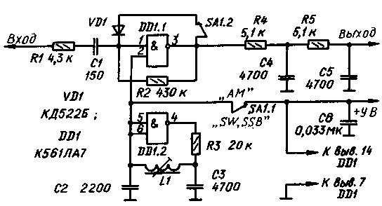
ENCYCLOPEDIA OF RADIO ELECTRONICS AND ELECTRICAL ENGINEERING AM, CW and SSB detector on a chip. Encyclopedia of radio electronics and electrical engineering
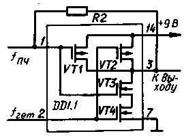
Encyclopedia of radio electronics and electrical engineering / radio reception Along with the telegraph and single-sideband modulation, amplitude modulation remains popular, especially among beginner radio amateurs on the 160 m band. Therefore, the creation of a simple combined detector is a very urgent task. Below is a simple AM, CW, SSB detector assembled on just one digital chip (Fig. 1). It uses two logical elements 2I-NOT. Element DD1.1. - linear controlled (strobe) IF amplifier. The operation of this amplifier is illustrated in Fig. 2, which shows a simplified schematic diagram of a two-input logic element 2I-NOT of the K561 series.
In the "AM" mode, a high-level voltage is applied to one of the inputs of the element (to pin 2), the transistor VT2 is closed, and VT4 is open. Due to the action of the negative feedback through the resistor R2, the operating point of the transistors VT1 and VT3 goes to the linear section of the current-voltage characteristic, in other words, these transistors work as an IF signal amplifier. To detect AM signals, a diode is included in the negative feedback circuit, due to which it becomes non-linear and the node turns into an AM detector for an input voltage of more than 5 mV.
Resistor R2 also helps to reduce the non-linear distortion of the low-frequency output signal. Detector transfer coefficient - 1...2. The R4C4R5C5 filter suppresses the IF voltage at the output of the detector. Due to the presence of the diode VD1 in the negative feedback circuit, the input resistance of the detector is quite small (a few kiloohms), therefore, in order for the detector not to shunt the output of the IF amplifier, a resistor R1 is provided at the detector input. This resistor also prevents the detector from self-exciting if the IF amplifier load is inductive. In the "CW, SSB" mode, the diode is excluded from the negative feedback circuit of the DD1.1 element by the SA1 switch. At the same time, its contacts SA1.1 remove the voltage of logic 1 from the lower element DD1.1 according to the input circuit and both inputs of the DD1.2 element. As a result of the feedback action through the resistor R3 and the coil L1, the DD1.2 element enters the linear section of the characteristic and begins to generate oscillations at the resonance frequency of the C2L1C3 circuit. Resistor R3 also reduces the influence of the output resistance of the logic element on the generation frequency. Thus, the DD1.2 element works as a telegraph local oscillator. An alternating voltage will be supplied to the lower input of the DD1.1 element, so the element will act as a mixer. To explain the principle of its operation in this mode, one should refer again to Fig. 2. When there is a logic 1 level at the heterodyne input of the element, it, as in the "AM" mode, will work as an amplifier. LF signal with gain Kmax. When the level at this input changes to 0, the transistor VT2 will be open, VT4 will be closed, the output of the element will be level 1, and the gain will decrease to zero. Thus, the transfer coefficient of the OD1.1 element can be written as follows:
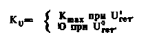
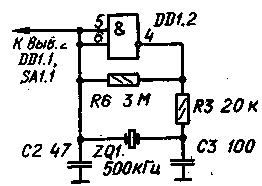
In other words, the element works similarly to a key mixer, the transmission coefficient of which changes in time with the local oscillator frequency. This allows you to use it to detect CW and SSB signals. The type of the detected SSB signal (selection of the upper or lower sideband) is set by changing the frequency of the telegraph local oscillator with the coil trimmer L1. The detector transmission coefficient in the "CW, SSB" mode is 0,5...1. The use of an LC circuit in a telegraph local oscillator is the reason for the relatively low stability of the generated frequency. Therefore, if it is possible to purchase a quartz resonator for the required frequency, then it is better to assemble a telegraph local oscillator according to the circuit shown in Fig. 3.
In the detector, you can use K561LA K561LA8, K561LA9 and similar microcircuits from the K 176, K564 series. Capacitors - KT, KLS, KM. Diode KD522B can be replaced with KD503B, as well as with any of the series D2, D9. Coil L1 was used ready-made - from the IF circuit of the "Giala" radio receiver. It can also be wound on the frame from the IF coils of the "Quartz" radio receiver - 63 coils of wire PEV-2 0,1 ... 0,12 (for a local oscillator frequency of 500 kHz for a frequency of 465 kHz, the number of turns should be increased by 10%). The detector does not require any adjustment and, with error-free installation and serviceable parts, it starts working immediately. The minimum input impedance of the detector is 5 kΩ, so it can be connected to the output of the IF amplifier instead of a conventional diode AM detector with the same input impedance. The input impedance of the 8H amplifier connected to the output of the detector must be at least 3.. 40 kOhm. The current consumed by the detector does not exceed 60-2 mA. Of course, this detector can only be used to detect CW and SSB signals. In this case, the diode VD1, the switch SA1 and the resistor R1 become redundant. The input impedance of the detector will increase to several tens of kiloohms, which will make it possible to connect it to the output of almost any IF amplifier. The voltage of the IF signal at the input of the detector must not exceed 500...600 mV, otherwise distortions that are noticeable to the ear may appear. Author: I. Nechaev, Kursk; Publication: N. Bolshakov, rf.atnn.ru
Artificial leather for touch emulation
15.04.2024 Petgugu Global cat litter
15.04.2024 The attractiveness of caring men
14.04.2024
▪ Single-chip controller SM2320 for portable external SSD ▪ Ultrabook Toshiba dynabook V632 has 13 hours battery life ▪ Ultra-processed foods increase risk of depression ▪ Artificial wood from the laboratory ▪ Specialized tablet for schools Galaxy Tab E
▪ section of the site Lecture notes, cheat sheets. Selection of articles ▪ Democritus article. Famous aphorisms ▪ article What is chalk? Detailed answer ▪ article MHD generator. Children's Science Lab ▪ article Perfuming toilet soaps. Simple recipes and tips ▪ article Coin in a decanter. Focus Secret
Comments on the article: Anatoly As long as the information is well presented, you can safely read, even consider device diagrams. Thank you!
Home page | Library | Articles | Website map | Site Reviews
www.diagram.com.ua |

 Leave your comment on this article: