Free technical library
PCB layout technology. Encyclopedia of radio electronics and electrical engineering

Encyclopedia of radio electronics and electrical engineering / Computers
 Comments on the article Comments on the article
|
GENERAL CONSIDERATIONS
|
|
Due to the significant differences between analog circuitry and digital circuitry, the analog part of the circuit must be separated from the rest of the circuit, and special methods and rules must be observed when wiring it. The effects of non-ideal PCB characteristics become especially noticeable in high-frequency analog circuits, but the general errors described in this article can affect the performance of devices operating even in the audio frequency range.
|
The intention of this article is to discuss common mistakes made by PCB designers, describe the impact of these mistakes on performance, and provide recommendations for resolving problems that arise. |
| |
|
Printed circuit board - circuit component
Only in rare cases can the printed circuit board of an analog circuit be routed so that the effects it introduces do not have any effect on the operation of the circuit. At the same time, any such impact can be minimized so that the characteristics of the device's analog circuitry are the same as those of the model and prototype.
Prototyping
Designers of digital circuits can correct small errors on the manufactured board by adding jumpers or, conversely, removing unnecessary conductors, making changes in the operation of programmable microcircuits, etc., moving on to the next development very soon. This is not the case for an analog circuit. Some of the common errors discussed in this article cannot be corrected by adding jumpers or removing excess wires. They can and will render the entire printed circuit board inoperable.
|
It is very important for a digital circuit designer using these correction methods to read and understand the material in this article well in advance of submitting the design to production. A little design attention and discussion of possible options will not only prevent the PCB from becoming a scrap, but also reduce the cost due to blunders in a small analog part of the circuit. Finding bugs and fixing them can waste hundreds of hours. Prototyping can reduce this time to one day or less. Breadboard all your analog circuits. |
| |
|
Sources of noise and interference
Noise and interference are the main elements that limit the quality characteristics of circuits. Interference can be either emitted by sources or induced on circuit elements. Analog circuitry is often found on a printed circuit board along with high-speed digital components, including digital signal processors (DSPs).
|
High-frequency logic signals create significant radio frequency interference (RFI). The number of sources of noise emission is enormous: key power supplies for digital systems, mobile phones, radio and television, power supplies for fluorescent lamps, personal computers, lightning discharges, etc. Even if the analog circuit is operating in the audio frequency range, RFI can create noticeable noise in the output signal. |
| |
|
PCB CATEGORIES
|
|
The choice of PCB design is an important factor in determining the mechanical performance of the device as a whole. For the manufacture of printed circuit boards, materials of various quality levels are used. The most suitable and convenient for the designer will be if the PCB manufacturer is nearby. In this case, it is easy to control the resistivity and dielectric constant - the main parameters of the printed circuit board material. Unfortunately, this is not enough, and knowledge of other parameters such as flammability, high temperature stability, and hygroscopicity is often required. These parameters can only be known by the manufacturer of the components used in the production of printed circuit boards.
Laminated materials are designated by the indices FR (flame resistant, resistance to ignition) and G. The material with the index FR-1 has the highest flammability, and FR-5 the least. Materials with indices G10 and G11 have special characteristics. The materials of printed circuit boards are given in Table. 1.
Do not use category FR-1 printed circuit board. There are many examples of FR-1 printed circuit boards that have suffered thermal damage from high power components. PCBs in this category are more like cardboard.
FR-4 is often used in the manufacture of industrial equipment, while FR-2 is used in the manufacture of household appliances. These two categories are industry standardized, and FR-2 and FR-4 circuit boards are often suitable for most applications. But sometimes the imperfection of the characteristics of these categories forces the use of other materials. For example, for very high frequency applications, PTFE and even ceramics are used as printed circuit board materials. However, the more exotic the PCB material, the higher the price can be.
When choosing a PCB material, pay special attention to its hygroscopicity, since this parameter can have a strong negative effect on the desired characteristics of the board - surface resistance, leakage, high-voltage insulating properties (breakdowns and sparks) and mechanical strength. Also pay attention to the operating temperature. Hot spots can be found in unexpected places, such as near large digital integrated circuits that switch at high frequency. If such areas are located directly below analog components, an increase in temperature can affect the characteristics of the analog circuit.
|
Table 1
|
|
|
|
FR-1
|
paper, phenolic composition: pressing and stamping at room temperature, high hygroscopicity
|
|
FR-2
|
paper, phenolic composition: applicable for single-sided printed circuit boards of household appliances, low water absorption coefficient
|
|
FR-3
|
paper, epoxy composition: developments with good mechanical and electrical characteristics
|
|
FR-4
|
fiberglass, epoxy composition: excellent mechanical and electrical properties
|
|
FR-5
|
fiberglass, epoxy composition: high strength at elevated temperatures, non-flammable
|
|
G10
|
fiberglass, epoxy composition: high insulating properties, the highest strength of fiberglass, low hygroscopicity
|
|
G11
|
fiberglass, epoxy composition: high flexural strength at elevated temperatures, high solvent resistance
|
Once the PCB material is selected, the thickness of the PCB foil must be determined. This parameter is primarily selected based on the maximum value of the flowing current. If possible, try to avoid using very thin foil.
|
| |
|
NUMBER OF LAYERS OF PRINTED BOARD
|
Depending on the overall circuit complexity and quality requirements, the designer must determine the number of PCB layers.
Single layer printed circuit boards
Very simple electronic circuits are made on single-sided boards using cheap foil materials (FR-1 or FR-2) and often have many jumpers, resembling double-sided boards. This way of creating printed circuit boards is recommended only for low-frequency circuits. For reasons to be described below, single-sided printed circuit boards are highly susceptible to interference. A good single-sided PCB is difficult to design for many reasons. Nevertheless, there are good boards of this type, but when developing them, you need to think a lot in advance.
Double layer printed circuit boards
At the next level are double-sided printed circuit boards, which in most cases use FR-4 as the substrate material, although sometimes FR-2 is also found. The use of FR-4 is more preferable, since holes are obtained from this material in printed circuit boards of better quality. Circuits on double-sided printed circuit boards are much easier to wire. in two layers, it is easier to route intersecting traces. However, trace crossing is not recommended for analog circuits. Where possible, the bottom layer (bottom) must be assigned to the ground polygon, and the rest of the signals should be routed in the upper layer (top). Using a landfill as a ground bus provides several benefits:
- the common wire is the most frequently connected wire in the circuit; so it makes sense to have a lot of common wire to simplify the wiring.
- increases the mechanical strength of the board.
- the resistance of all connections to the common wire is reduced, which, in turn, reduces noise and interference.
- the distributed capacitance for each circuit circuit is increased, helping to suppress radiated noise.
- the polygon, which is a screen, suppresses pickups emitted by sources located on the side of the polygon.
Double-sided printed circuit boards, despite all their advantages, are not the best, especially for small-signal or high-speed circuits. In general, the PCB thickness, i.e. the distance between the plating layers is 1,5 mm, which is too much to fully realize some of the advantages of a two-layer printed circuit board, given above. The allocated capacity, for example, is too small due to such a large spacing.
Multilayer printed circuit boards
Responsible circuit design requires multilayer printed circuit boards (MPBs). Some reasons for their use are obvious:
- the same convenient as for the common wire bus, power bus wiring; if polygons on a separate layer are used as power buses, then it is quite simple to supply power to each element of the circuit using vias;
- signal layers are freed from power rails, which facilitates the wiring of signal conductors;
- distributed capacitance appears between the ground and power polygons, which reduces high-frequency noise.
|
In addition to these reasons for using multilayer printed circuit boards, there are other less obvious ones:
- better suppression of electromagnetic (EMI) and radio frequency (RFI) interference due to the reflection effect (image plane effect), known since the time of Marconi. When a conductor is placed close to a flat conducting surface, most of the return high frequency currents will flow in the plane directly below the conductor. The direction of these currents will be opposite to the direction of currents in the conductor. Thus, the reflection of the conductor in the plane creates a signal transmission line. Since the currents in the conductor and in the plane are equal in magnitude and opposite in direction, some reduction in radiated interference is created. Reflection effect works effectively only with non-breaking solid polygons (they can be both ground polygons and food polygons). Any breach of integrity will result in a reduction in interference suppression.
- reducing the overall cost in small-scale production. Even though multilayer printed circuit boards are more expensive to manufacture, their possible emission is less than that of single and double layer boards. Therefore, in some cases, the use of only multilayer boards will allow you to meet the requirements for radiation set during the development, and not to carry out additional tests and tests. The use of MFP can reduce the level of radiated noise by 20 dB compared to two-layer boards.
Layer order
For inexperienced designers, there is often some confusion about the optimal order of PCB layers. Take for example a 4-layer chamber containing two signal layers and two polygon layers - a ground layer and a power layer. What is the best layer order? Signal layers between polygons that will serve as screens? Or to make the polygon layers internal to reduce the interference of the signal layers?
An important thing to keep in mind when solving this issue is that often the location of the layers doesn't really matter, because the components are still located on the outer layers, and the buses that feed signals to their terminals sometimes pass through all the layers. Therefore, any screen effects are only a compromise. In this case, it is better to take care of creating a large distributed capacity between the power and ground polygons, placing them in the inner layers.
Another advantage of having the signal layers on the outside is the availability of signals for testing, as well as the possibility of modifying connections. Anyone who has ever changed the connections of conductors located in the inner layers will appreciate this opportunity.
For printed circuit boards with more than four layers, it is a general rule to place high-speed signal traces between the ground and power planes, and leave the outer layers for low-frequency ones.
|
| |
|
GROUNDING
|
Good grounding is a common requirement for a rich, layered system. And it should be planned from the first step of design development.Basic rule: division of the land.
Dividing the ground into analog and digital parts is one of the simplest and most effective methods of noise suppression. One or more layers of a multi-layer printed circuit board is usually allocated under a layer of ground planes. If the developer is not very experienced or careless, then the ground of the analog part will be directly connected to these polygons, i.e. the analog return current will use the same circuit as the digital return current. Auto breeders work in much the same way and unite all the lands together.
If a previously designed printed circuit board with a single ground polygon combining analog and digital grounds is subjected to processing, then it is necessary to physically separate the grounds on the board first (after this operation, the operation of the board becomes almost impossible). After that, all connections are made to the analog ground plane of the analog circuit components (analog ground is formed) and to the digital ground plane of the digital circuit components (digital ground is formed). And only after that, the digital and analog grounds are combined in the source.
Other land formation rules:
- The power and ground rails must be at the same AC potential., which implies the use of decoupling capacitors and distributed capacitance.
- Avoid overlapping analog and digital polygons (Fig. 1). Position the analog power rails and polygons above the analog ground polygon (similarly for digital power rails). If there is an overlap between the analog and digital ranges at any point, the distributed capacitance between the overlapping areas will create AC coupling, and the noise from the operation of the digital components will enter the analog circuit. Such overlaps will invalidate polygon isolation.
- Separation does not mean electrical isolation of analog from digital ground (Figure 2). They must be connected together in some, preferably one, low-impedance node. A proper grounded system has only one ground, which is the ground terminal for AC mains powered systems or the common ground for DC powered systems (such as a battery). All signal and power currents in this circuit must return to this ground at a single point, which will serve as the system ground. Such a point can be the output of the device case. It is important to understand that ground loops can form when connecting the circuit ground to multiple points on the package. The creation of a single common ground point is one of the most difficult aspects of system design.
- If possible, separate the terminals of the connectors intended to carry return currents - the return currents should only be combined at the system ground point. The aging of the connector contacts, as well as the frequent disconnection of their mating parts, leads to an increase in the resistance of the contacts, therefore, for more reliable operation, it is necessary to use connectors with a certain number of additional pins. Complex digital printed circuit boards have many layers and contain hundreds or thousands of conductors. Adding another conductor rarely creates a problem, unlike adding additional connector pins. If this fails, then it is necessary to create two return current conductors for each power circuit on the board, taking special precautions.
- It is important to separate the digital signal lines from the places on the PCB where the analog components of the circuit are located. This involves isolation (shielding) by polygons, short analog signal paths, and careful placement of passive components with high-speed digital and critical analog busses adjacent. Digital signal busses should be routed around analog component areas and not overlap with analog ground and analog power busses and polygons. If this is not done, then the development will contain a new unforeseen element - an antenna, the radiation of which will affect high-impedance analog components and conductors (Fig. 3).
|
Almost all clock signals are high enough frequency signals that even small capacitances between traces and polygons can create significant coupling. It must be remembered that not only the main clock frequency can cause a problem, but also its higher harmonics.
- It is a good concept to place the analog part of the circuit close to the board's I/O connections. Digital PCB designers using high-power integrated circuits often tend to run busbars 1 mm wide and several centimeters long to connect analog components, believing that low trace resistance will help eliminate crosstalk. What you end up with is an extended film capacitor, which will pick up spurious signals from digital components, digital ground, and digital power, exacerbating the problem.
An example of good component placement
Figure 4 shows a possible layout of all components on the board, including the power supply. Three separate and isolated ground/power planes are used here: one for the source, one for the digital circuit, and one for the analog circuit. The ground and power circuits of the analog and digital parts are combined only in the power supply. High-frequency noise is filtered out in the supply circuits by chokes. In this example, the high frequency signals of the analog and digital parts are separated from each other. Such a design has a very high probability of a favorable outcome, since it ensures good placement of components and adherence to the rules of separation of circuits.  There is only one case where analog and digital signals need to be combined over an analog ground area. Analog-to-digital and digital-to-analog converters are housed in housings with analog and digital ground pins. Considering the previous considerations, it can be assumed that the digital ground pin and the analog ground pin should be connected to the digital and analog ground buses, respectively. However, this is not true in this case.
The pin names (analog or digital) refer only to the internal structure of the converter, to its internal connections. In the circuit, these pins should be connected to the analog ground bus. The connection can also be made inside the integrated circuit, however, it is rather difficult to obtain a low resistance of such a connection due to topological limitations. Therefore, when using converters, an external connection of the analog and digital ground pins is assumed. If this is not done, then the parameters of the microcircuit will be much worse than those given in the specification.
It must be taken into account that the digital elements of the converter can degrade the quality characteristics of the circuit, introducing digital noise into the analog ground and analog power circuits. The design of the converters takes this negative impact into account so that the digital part consumes as little power as possible. In this case, interference from switching logic elements is reduced. If the digital outputs of the converter are not heavily loaded, then internal switching usually does not cause much problems. When designing a printed circuit board containing an ADC or DAC, due consideration must be given to decoupling the converter's digital power to analog ground.
|
| |
|
FREQUENCY CHARACTERISTICS OF PASSIVE COMPONENTS
|
Proper selection of passive components is essential for the correct operation of analog circuits. Begin your design development by carefully considering the high frequency characteristics of passive components and pre-positioning and arranging them on the board sketch.
A large number of designers completely ignore the frequency limitations of passive components when used in analog circuitry. These components have limited frequency ranges and their operation outside the specified frequency range can lead to unpredictable results. One might think that this discussion is only about high-speed analog circuits. However, this is far from being the case - high-frequency signals affect the passive components of low-frequency circuits quite strongly through radiation or direct connection through conductors. For example, a simple low-pass filter on an op-amp can easily turn into a high-pass filter when high frequency is applied to its input.
Resistors
The high frequency characteristics of the resistors can be represented by the equivalent circuit shown in Figure 5.
Usually three types of resistors are used: 1) wire, 2) carbon composite and 3) film. It doesn't take much imagination to understand how a wirewound resistor can turn into an inductance, since it is a coil of high resistance metal wire. Most electronic device designers have no idea about the internal structure of film resistors, which are also a coil, albeit made of a metal film. Therefore, film resistors also have an inductance that is less than that of wirewound resistors. Film resistors with a resistance of no more than 2 kOhm can be freely used in high-frequency circuits. The terminals of the resistors are parallel to each other, so there is a noticeable capacitive coupling between them. For high resistance resistors, terminal capacitance will reduce the overall impedance at high frequencies.
Capacitors
The high frequency characteristics of capacitors can be represented by the equivalent circuit shown in Figure 6. 
Capacitors in analog circuits are used as decoupling and filtering components. For an ideal capacitor, the reactance is determined by the following formula:
Therefore, a 10µF electrolytic capacitor will have a resistance of 1,6Ω at 10kHz and 160µΩ at 100MHz. Is it so?
In fact, no one has ever seen an electrolytic capacitor with a reactance of 160 µΩ. The plates of film and electrolytic capacitors are twisted foil layers that create parasitic inductance. The self-inductance effect of ceramic capacitors is much less, which allows them to be used when operating at high frequencies. In addition, capacitors have a leakage current between the plates, which is equivalent to a resistor connected in parallel with their terminals, which adds its parasitic effect to the effect of the series-connected resistance of the terminals and plates. In addition, the electrolyte is not a perfect conductor. All these resistances add up to create an equivalent series resistance (ESR). Capacitors used as decouplers must have low ESR, since series resistance limits the effectiveness of ripple and noise suppression. Increasing the operating temperature increases the equivalent series resistance quite significantly and can degrade the performance of the capacitor. Therefore, if an aluminum electrolytic capacitor is to be used at an elevated operating temperature, the appropriate type of capacitor (105°C) must be used.
The capacitor leads also contribute to the parasitic inductance. For small capacitance values, it is important to keep lead lengths short. The combination of parasitic inductance and capacitance can create a resonant circuit. Assuming the leads have an inductance of about 8nH per centimeter, a 0,01uF capacitor with leads one centimeter long will have a resonant frequency of about 12,5MHz. This effect is known to engineers who developed electronic vacuum devices decades ago. Anyone who restores antique radios and is unaware of this effect faces many problems.
When using electrolytic capacitors, the correct connection must be observed. The positive terminal must be connected to a more positive DC potential. Incorrect connection causes DC current to flow through the electrolytic capacitor, which can damage not only the capacitor itself, but also part of the circuit.
In rare cases, the DC potential difference between two points in a circuit can reverse sign. This requires the use of non-polar electrolytic capacitors, the internal structure of which is equivalent to two polar capacitors connected in series.
inductance
The high frequency characteristics of inductors can be represented by the equivalent circuit shown in Figure 7.
The reactance of an inductor is described by the following formula:
Therefore, a 10 mH inductor will have a reactance of 628 ohms at 10 kHz and a reactance of 100 MΩ at 6,28 MHz. Right?
|
In reality, there is no 6,28 MΩ inductor. The nature of parasitic resistance is easy to understand - the turns of the coil are made of wire that has some resistance per unit length. Parasitic capacitance is more difficult to perceive until one takes into account the fact that the next turn of the coil is located close to the previous one, and capacitive coupling occurs between closely spaced conductors. Parasitic capacitance limits the upper operating frequency. Small wirewound inductors start to become inefficient in the 10...100 MHz range.
Printed circuit board
The printed circuit board itself has the characteristics of the passive components discussed above, although not so obvious.
The pattern of conductors on a printed circuit board can be both a source and a receiver of interference. Good wiring reduces the sensitivity of the analog circuit to radiated sources.
The printed circuit board is susceptible to radiation because the conductors and leads of the components form a kind of antenna. Antenna theory is a fairly complex subject to study and is not covered in this article. However, some basics are given here.
A bit of antenna theory
One of the main types of antennas is the rod or straight conductor. Such an antenna works because a straight conductor has parasitic inductance and therefore can concentrate and trap radiation from external sources. The total impedance of a straight conductor has a resistive (active) and an inductive (reactive) component:
At direct current or low frequencies, the active component predominates. As the frequency increases, the reactive component becomes more and more significant. In the range from 1 kHz to 10 kHz, the inductive component starts to take effect, and the conductor is no longer a low-resistance connector, but rather acts as an inductor.
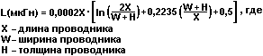
The formula for calculating the inductance of a PCB conductor is as follows:
Typically, PCB traces have values between 6 nH and 12 nH per centimeter of length. For example, a 10 cm conductor has a resistance of 57 mΩ and an inductance of 8 nH per cm. At 100 kHz, the reactance becomes 50 mΩ, and at higher frequencies the conductor will be an inductance rather than a resistance.
The whip antenna rule states that it begins to noticeably interact with the field at its length of about 1/20 of the wavelength, and the maximum interaction occurs at the length of the pin, equal to 1/4 of the wavelength. Therefore, the 10 cm conductor from the example in the previous paragraph will start to become a pretty good antenna at frequencies above 150 MHz. It must be remembered that despite the fact that the clock generator of a digital circuit may not operate at a frequency higher than 150 MHz, higher harmonics are always present in its signal. If the printed circuit board contains components with pin leads of considerable length, then such pins can also serve as antennas.
The other main type of antenna is the loop antenna. The inductance of a straight conductor increases greatly when it bends and becomes part of an arc. Increasing inductance lowers the frequency at which the antenna begins to interact with the field lines.
Experienced PCB designers who are fairly well versed in the theory of loop antennas know not to create loops for critical signals. Some designers, however, do not think about this, and the return and signal current conductors in their circuits are loops. The creation of loop antennas is easy to show with an example (Fig. 8). In addition, the creation of a slot antenna is shown here.
Let's consider three cases:
Option A is an example of bad design. It does not use the analog ground polygon at all. The loop circuit is formed by a ground and signal conductor. When a current passes, an electric field and a magnetic field perpendicular to it arise. These fields form the basis of a loop antenna. The loop antenna rule states that for maximum efficiency, the length of each conductor should be equal to half the wavelength of the received radiation. However, one should not forget that even at 1/20 of the wavelength, the loop antenna is still quite effective.
Option B is better than Option A, but there is a gap in the polygon, probably to create a specific place for the signal wires to be routed. The signal and return current paths form a slot antenna. Other loops are formed in the cutouts around the chips.
Option B is an example of a better design. The signal and return current paths overlap, negating the efficiency of the loop antenna. Note that this option also has cutouts around the ICs, but they are separated from the return current path.
The theory of reflection and matching of signals is close to the theory of antennas.
When the PCB conductor is rotated through 90°, reflections can occur. This is mainly due to the change in the width of the current path. At the top of the corner, the trace width increases by a factor of 1.414, which leads to a mismatch in the characteristics of the transmission line, especially the distributed capacitance and the intrinsic inductance of the trace. Quite often it is necessary to rotate a trace 90° on a PCB. Many modern CAD packages allow you to smooth the corners of the drawn paths or draw the paths in the form of an arc. Figure 9 shows two steps to improve the corner shape. Only the last example keeps the trace width constant and minimizes reflections.
Tip for experienced PCB layoutrs: leave the smoothing procedure to the last stage of work before creating droplets and pouring polygons. Otherwise, the CAD package will take longer to smooth due to more complex calculations.
|
|
| |
|
PARASITE EFFECTS OF THE PRINTED BOARD
|
PCB traces on different layers are capacitively coupled when they cross. Sometimes this can create a problem. Conductors stacked on top of each other on adjacent layers create a long film capacitor. The capacitance of such a capacitor is calculated according to the formula shown in Figure 10.
For example, a printed circuit board may have the following parameters:
- 4 layers; signal and ground polygon layer are adjacent,
- interlayer interval - 0,2 mm,
- conductor width - 0,75 mm,
- conductor length - 7,5 mm.
Typical ER value for FR-4 is 4.5.
Substituting all the values into the formula, we get the capacitance value between these two buses, equal to 1,1 pF. Even such a seemingly small capacity is unacceptable for some applications. Figure 11 illustrates the effect of a 1 pF capacitance when connected to the inverting input of a high frequency op amp.
It can be seen that the output signal amplitude doubles at frequencies close to the upper limit of the OS frequency range. This, in turn, can lead to generation, especially at antenna operating frequencies (above 180 MHz).
This effect gives rise to numerous problems, for which, nevertheless, there are many ways. The most obvious of these is the reduction in the length of the conductors. Another way is to reduce their width. There is no reason to use a conductor of this width to feed the signal to the inverting input, since Very little current flows through this conductor. Reducing the trace length to 2,5 mm and the width to 0,2 mm will reduce the capacitance to 0,1 pF, and such a capacitance will no longer lead to such a significant increase in the frequency response. Another way to solve it is to remove part of the polygon under the inverting input and the conductor coming up to it.
The inverting input of an op amp, especially a high speed op amp, is highly prone to oscillating in high gain circuits. This is due to the unwanted capacitance of the op-amp input stage. Therefore, it is extremely important to reduce parasitic capacitance and place the feedback components as close to the inverting input as possible. If, despite the measures taken, the amplifier is excited, then it is necessary to proportionally reduce the resistance of the feedback resistors to change the resonant frequency of the circuit. An increase in resistors can also help, however, much less often, because. the excitation effect also depends on the impedance of the circuit. When changing the feedback resistors, one should not forget about changing the capacitance of the correction capacitor. Also, we must not forget that with a decrease in the resistance of the resistors, the power consumption of the circuit increases.
|
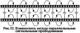
The width of PCB traces cannot be reduced indefinitely. The limiting width is determined by both the technological process and the thickness of the foil. If two conductors pass close to each other, then a capacitive and inductive coupling is formed between them (Fig. 12).
The relationships describing these parasitic effects are complex enough to be given in this article, but they can be found in the literature on transmission lines and striplines.
Signal wires should not be run parallel to each other, except in the case of differential or microstrip wiring. The gap between the conductors must be at least three times the width of the conductors.
Capacitance between traces in analog circuits can be problematic for large resistor values (several MΩ). The relatively large capacitive coupling between the inverting and non-inverting inputs of an op-amp can easily cause the circuit to self-excite.
Whenever, when laying out a printed circuit board, it becomes necessary to create a via, i.e. interconnection (Fig. 13), it must be remembered that parasitic inductance also arises. With a hole diameter after plating d and a channel length h, the inductance can be calculated using the following approximate formula:
For example, with d=0,4 mm and h=1,5 mm (quite common values), the inductance of the hole is 1,1 nH.
Keep in mind that the inductance of the hole, together with the same parasitic capacitance, form a resonant circuit, which can be affected when working at high frequencies. The hole's intrinsic inductance is quite low and the resonant frequency is somewhere in the gigahertz range, but if the signal is forced to pass through multiple vias along its path, their inductances add up (in series connection) and the resonant frequency drops. Conclusion: try to avoid a large number of vias when routing the critical high-frequency conductors of analog circuits. Another negative phenomenon is that with a large number of vias in the ground polygon, loops can be created. The best analog wiring - all signal conductors are on the same PCB layer.
In addition to the parasitic effects discussed above, there are also those that are associated with an insufficiently clean surface of the board.
Remember that if there are large resistances in the circuit, then special attention should be paid to cleaning the board. Flux residues and contaminants must be removed during the final stages of PCB fabrication. Recently, when mounting printed circuit boards, water-soluble fluxes are often used. Being less harmful, they are easily removed with water. But at the same time, washing the board with insufficiently clean water can lead to additional contamination, which worsens the dielectric characteristics. Therefore, it is very important to clean the PCB with high impedance circuitry with fresh distilled water.
|
| |
|
SIGNAL INTERCOUPLING
|
As already noted, noise can enter the analog part of the circuit through the power circuits. To reduce such interference, decoupling (blocking) capacitors are used to reduce the local impedance of the power buses.
If you need to separate a printed circuit board that has both analog and digital parts, then you need to have at least a small idea of \uXNUMXb\uXNUMXbthe electrical characteristics of logic elements.
A typical output stage of a logic element contains two transistors connected in series with each other, as well as between the power and ground circuits (Fig. 14).
These transistors ideally operate strictly in antiphase, i.e. when one of them is open, then at the same time the second one is closed, generating either a logical one or a logical zero signal at the output. In the steady-state logic state, the power consumption of the logic element is small.
The situation changes dramatically when the output stage switches from one logic state to another. In this case, for a short period of time, both transistors can be opened simultaneously, and the output stage supply current increases greatly, since the resistance of the section of the current path from the power bus to the ground bus through two series-connected transistors decreases. The power consumption increases abruptly and then also decreases, which leads to a local change in the supply voltage and the appearance of a sharp, short-term change in current. Such current changes result in the emission of RF energy. Even on a relatively simple printed circuit board, there may be dozens or hundreds of considered output stages of logic elements, so the total effect of their simultaneous operation can be very large.
It is impossible to accurately predict the frequency range over which these current surges will occur, since the frequency of their occurrence depends on many factors, including the propagation delay of switching transistors in the logic element. The delay, in turn, also depends on many random causes that occur during the production process. Switching noise has a broadband harmonic distribution over the entire range. To suppress digital noise, there are several methods, the application of which depends on the spectral distribution of the noise.
Table 2 lists the maximum operating frequencies for common capacitor types.
Table 2
|
|
|
|
aluminum electrolytic
|
100 kHz
|
|
tantalum electrolytic
|
1 MHz
|
|
mica
|
500 MHz
|
|
ceramic
|
1 GHz
|
|
From the table it is obvious that tantalum electrolytic capacitors are used for frequencies below 1 MHz, at higher frequencies ceramic capacitors should be used. It must be remembered that capacitors have their own resonance and the wrong choice of them can not only not help, but also exacerbate the problem. Figure 15 shows typical self-resonances of two general purpose capacitors, a 10 µF tantalum electrolytic and a 0,01 µF ceramic.
Actual specifications may vary from manufacturer to manufacturer and even from lot to lot from the same manufacturer. It is important to understand that for the capacitor to work effectively, the frequencies it suppresses must be in a lower range than the self-resonant frequency. Otherwise, the nature of the reactance will be inductive, and the capacitor will no longer work effectively.
Make no mistake that a single 0,1uF capacitor will reject all frequencies. Small capacitors (10 nF or less) can work more efficiently at higher frequencies.
IC Power Decoupling
Integrated circuit power decoupling to suppress high frequency noise consists of one or more capacitors connected between the power and ground pins. It is important that the conductors connecting the leads to the capacitors are kept short. If this is not the case, then the self-inductance of the conductors will play a significant role and negate the benefits of using decoupling capacitors.
A decoupling capacitor must be connected to each package of the microcircuit, regardless of whether there are 1, 2 or 4 opamps inside the package. If the op-amp is powered by a bipolar supply, then it goes without saying that decoupling capacitors must be located at each power pin. The capacitance value must be carefully chosen depending on the type of noise and interference present in the circuit.
In particularly difficult cases, it may be necessary to add an inductor connected in series with the power output. The inductance should be placed before, not after, the capacitors.
Another, cheaper way is to replace the inductance with a low resistance resistor (10 ... 100 ohms). In this case, together with the decoupling capacitor, the resistor forms a low-frequency filter. This method reduces the supply range of the op-amp, which also becomes more dependent on power consumption.
Usually, to suppress low-frequency noise in power circuits, it is sufficient to use one or more aluminum or tantalum electrolytic capacitors at the power input connector. An additional ceramic capacitor will suppress high frequency noise from other boards.
|
| |
|
INPUT AND OUTPUT DEPOSIT
|
Many noise problems result from directly connecting input and output pins. As a result of the high-frequency limitations of passive components, the circuit's response to exposure to high-frequency noise can be quite unpredictable.
In a situation where the frequency range of the induced noise is significantly different from the frequency range of the circuit, the solution is simple and obvious - to place a passive RC filter to suppress high-frequency noise. However, when using a passive filter, one must be careful: its characteristics (due to the imperfection of the frequency characteristics of passive components) lose their properties at frequencies that are 100 ... 1000 times higher than the cutoff frequency (f3db). When using series-connected filters tuned to different frequency ranges, the higher-pass filter should be closest to the interferer. Ferrite inductors can also be used for noise suppression; they retain the inductive nature of the resistance up to a certain specific frequency, and above their resistance becomes active.
|
The interference on the analog circuit can be so great that it is possible to get rid of (or at least reduce) it only by using screens. To work effectively, they must be carefully designed so that the frequencies that cause the most problems cannot enter the circuit. This means that the shield must not have holes or cutouts larger than 1/20 of the wavelength of the shielded radiation. It is a good idea to allow enough space for the intended screen from the very beginning of the PCB design. When using a shield, you can additionally use ferrite rings (or beads) for all connections to the circuit.
|
| |
|
OP-AMP BODIES
|
One case usually houses one, two or four operational amplifiers (Fig. 16).
A single op-amp often also has additional inputs, for example to adjust the bias voltage. Dual and quad op amps have only inverting and non-inverting inputs and outputs. Therefore, if you need to have additional adjustments, you must use single operational amplifiers. When using auxiliary outputs, it must be remembered that they are auxiliary inputs in their structure, therefore, they must be managed carefully and in accordance with the manufacturer's recommendations.
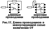
In a single op-amp, the output is located on the opposite side of the inputs. This can make it difficult to operate the amplifier at high frequencies due to the length of the feedback wires. One way to overcome this is to place the amplifier and feedback components on opposite sides of the PCB. This, however, results in at least two additional holes and cutouts in the ground polygon. Sometimes it is worth using a dual op-amp to solve this problem, even if the second amplifier is not used (and its outputs must be connected properly). Figure 17 illustrates the shortening of the feedback loop wires for an inverting connection.
Dual op amps are especially common in stereo amplifiers, and quad op amps in multi-stage filter circuits. However, this has a rather significant downside. Although current technology provides decent isolation between the signals of amplifiers located on the same silicon chip, there is still some crosstalk between them. If it is necessary to have a very small amount of such interference, then it is necessary to use single operational amplifiers. Crosstalk does not only occur with dual or quad amplifiers. Their source can be a very close location of the passive components of different channels.
Dual and quad op amps, in addition to the above, allow for tighter mounting. Separate amplifiers are, as it were, mirrored relative to each other (Fig. 18). |
Figures 17 and 18 do not show all of the connections required for normal operation, such as a midrange driver with a single supply. Figure 19 shows a diagram of such a driver when using a quad amplifier.
The diagram shows all the necessary connections for the implementation of three independent inverting stages. It is necessary to pay attention to the fact that the conductors of the half-voltage driver are located directly under the integrated circuit package, which makes it possible to reduce their length. This example illustrates not how it should be, but what should be done. The mid-level voltage, for example, could be the same for all four amplifiers. Passive components can be appropriately sized. For example, size 0402 planar components match the pin spacing of a standard SO package. This allows very short conductor lengths for high frequency applications.
Operational amplifier package types mainly include DIP (dual-in-line) and SO (small-outline). As the package size decreases, so does the lead spacing, allowing the use of smaller passive components. Reducing the size of the circuit as a whole reduces parasitic inductances and allows operation at higher frequencies. However, this also results in stronger crosstalk due to increased capacitive coupling between components and conductors.
|
| |
|
VOLUMETRIC AND SURFACE MOUNTING
|
When placing operational amplifiers in DIP packages and passive components with wire leads, the presence of vias on the printed circuit board is required for their installation. Such components are currently used when there are no special requirements for PCB dimensions; they are usually cheaper, but the cost of the printed circuit board increases during the manufacturing process due to drilling additional holes for component leads.
In addition, when using add-on components, the dimensions of the board and the length of the conductors increase, which does not allow the circuit to operate at high frequencies. The vias have their own inductance, which also imposes restrictions on the dynamic characteristics of the circuit. Therefore, plug-in components are not recommended for high-frequency circuits or for analog circuits located near high-speed logic circuits.
|
Some designers, in an attempt to reduce the length of the conductors, place the resistors vertically. At first glance, it may seem that this reduces the length of the route. However, this increases the current path through the resistor, and the resistor itself is a loop (coil of inductance). The radiating and receiving capacity increases many times over.
Surface mount does not require a hole for each pin of the component. However, there are problems when testing a circuit, and you have to use vias as test points, especially when using small-scale components.
|
| |
|
UNUSED OU SECTIONS
|
When using dual and quad op amps in the circuit, some of their sections may remain unused and must be connected correctly in this case. Incorrect connection can lead to an increase in power consumption, more heat and more noise used in the same package of op-amps. The outputs of unused operational amplifiers can be connected as shown in fig. 20a. Connecting pins with additional components (Fig. 20b) will make it easy to use this op-amp during commissioning.
|
|
| |
|
CONCLUSION
|
Keep the following key points in mind and keep them in mind when designing and wiring analog circuits.Are common:
- think of the printed circuit board as an electrical circuit component;
- have an idea and understanding of the sources of noise and interference;
- model and layout circuits.
Printed circuit board:
- use printed circuit boards only from high-quality material (for example, FR-4);
- circuits made on multilayer printed circuit boards are 20 dB less susceptible to external interference than circuits made on two-layer boards;
- use separate, non-overlapping polygons for different lands and feeds;
- place the ground and power polygons on the inner layers of the PCB.
Components:
- be aware of the frequency limitations introduced by the board's passive components and traces;
- try to avoid vertical placement of passive components in high speed circuits;
- for high-frequency circuits, use components designed for surface mounting;
- conductors should be the shorter the better;
- if a longer conductor length is required, then reduce its width;
- unused leads of active components must be properly connected.
|
Wiring:
- place the analog circuit near the power connector;
- never route wires carrying logic signals through the analog area of the board, and vice versa;
- make the conductors suitable for the inverting input of the op-amp short;
- make sure that the conductors of the inverting and non-inverting inputs of the op-amp are not parallel to each other for a long distance;
- try to avoid using extra vias, because their own inductance can lead to additional problems;
- do not run conductors at right angles and smoothen the tops of the corners if possible.
Interchange:
- use the correct types of capacitors to suppress noise in power circuits;
- to suppress low-frequency interference and noise, use tantalum capacitors at the power input connector;
- to suppress high-frequency interference and noise, use ceramic capacitors at the power input connector;
- use ceramic capacitors at each power output of the microcircuit; if necessary, use several capacitors for different frequency ranges;
- if excitation occurs in the circuit, then it is necessary to use capacitors with a smaller capacitance value, and not a larger one;
- in difficult cases in power circuits, use series-connected resistors of small resistance or inductance;
- analog power decoupling capacitors should only be connected to analog ground, not digital ground.
|
Publication: cxem.net
 See other articles Section Computers. See other articles Section Computers.
Read and write useful comments on this article.
<< Back
 Latest news of science and technology, new electronics: Latest news of science and technology, new electronics:
Artificial leather for touch emulation
15.04.2024
In a modern technology world where distance is becoming increasingly commonplace, maintaining connection and a sense of closeness is important. Recent developments in artificial skin by German scientists from Saarland University represent a new era in virtual interactions. German researchers from Saarland University have developed ultra-thin films that can transmit the sensation of touch over a distance. This cutting-edge technology provides new opportunities for virtual communication, especially for those who find themselves far from their loved ones. The ultra-thin films developed by the researchers, just 50 micrometers thick, can be integrated into textiles and worn like a second skin. These films act as sensors that recognize tactile signals from mom or dad, and as actuators that transmit these movements to the baby. Parents' touch to the fabric activates sensors that react to pressure and deform the ultra-thin film. This ... >>
Petgugu Global cat litter
15.04.2024
Taking care of pets can often be a challenge, especially when it comes to keeping your home clean. A new interesting solution from the Petgugu Global startup has been presented, which will make life easier for cat owners and help them keep their home perfectly clean and tidy. Startup Petgugu Global has unveiled a unique cat toilet that can automatically flush feces, keeping your home clean and fresh. This innovative device is equipped with various smart sensors that monitor your pet's toilet activity and activate to automatically clean after use. The device connects to the sewer system and ensures efficient waste removal without the need for intervention from the owner. Additionally, the toilet has a large flushable storage capacity, making it ideal for multi-cat households. The Petgugu cat litter bowl is designed for use with water-soluble litters and offers a range of additional ... >>
The attractiveness of caring men
14.04.2024
The stereotype that women prefer "bad boys" has long been widespread. However, recent research conducted by British scientists from Monash University offers a new perspective on this issue. They looked at how women responded to men's emotional responsibility and willingness to help others. The study's findings could change our understanding of what makes men attractive to women. A study conducted by scientists from Monash University leads to new findings about men's attractiveness to women. In the experiment, women were shown photographs of men with brief stories about their behavior in various situations, including their reaction to an encounter with a homeless person. Some of the men ignored the homeless man, while others helped him, such as buying him food. A study found that men who showed empathy and kindness were more attractive to women compared to men who showed empathy and kindness. ... >>
| Random news from the Archive Car tires with living moss inside
19.03.2018
Goodyear presented at the next Geneva Motor Show a very unusual concept - Oxygene tires with living moss inside, which absorbs carbon dioxide and produces oxygen.
It is assumed that such tires will be able to generate energy through photosynthesis. As planned by the company, they will absorb CO2 from the air and moisture from the road surface, nourishing the moss inside the sidewall, and produce oxygen. Goodyear estimates that in a city the size of Paris with about 2,5 million cars on the road, the widespread use of Oxygene tires will generate about 3 tons of oxygen and absorb more than 000 tons of carbon dioxide per year.
In addition, the concept tires use the resulting energy to power the internal electronics, in particular the built-in sensors and the data processing unit. It is also noted that the tires will use Li-Fi technology, which will allow them to "communicate" with other cars and road infrastructure. The treads, according to Goodyear, will be 3D printed from rubber powder obtained from recycled tyres.
|
Other interesting news:
▪ Chinese electronics will be assembled in the US
▪ The magnetic moment of the muon is the fifth force of nature
▪ The effect of physical education on DNA
▪ Edible battery
▪ Memories make us forget
News feed of science and technology, new electronics
Interesting materials of the Free Technical Library:
▪ section of the Electrician website. PTE. Article selection
▪ Article Old horseradish. Popular expression
▪ article What makes people laugh? Detailed answer
▪ article Straight knot. Travel Tips
▪ article Diagnostic tool for car engine with BOSCH controller. Encyclopedia of radio electronics and electrical engineering
▪ article Automatic charger for Ni-Cd batteries. Encyclopedia of radio electronics and electrical engineering
Leave your comment on this article:
 All languages of this page All languages of this page
Home page | Library | Articles | Website map | Site Reviews

www.diagram.com.ua
2000-2024
|


 Arabic
 Bengali
 Chinese
 English
 French
 German
 Hebrew
 Hindi
Hindi Italian
 Japanese
 Korean
 Malay
Malay Polish
 Portuguese
 Spanish
 Turkish
 Ukrainian
 Vietnamese