|
|


 Arabic
 Bengali
 Chinese
 English
 French
 German
 Hebrew
 Hindi
Hindi Italian
 Japanese
 Korean
 Malay
Malay Polish
 Portuguese
 Spanish
 Turkish
 Ukrainian
 Vietnamese
|
ENCYCLOPEDIA OF RADIO ELECTRONICS AND ELECTRICAL ENGINEERING Calculation of transistor amplifiers. Encyclopedia of radio electronics and electrical engineering
Encyclopedia of radio electronics and electrical engineering / Beginner radio amateur Transistors, as soon as they appeared, quickly won a dominant place in amplifying technology, and there are several reasons for this. Transistors do not have a filament, which means that they do not require power to heat it, they work well at low supply voltage, they are well matched with low-resistance loads (for example, dynamic loudspeaker heads), they are durable and reliable. Unlike tubes, the characteristics of transistors are markedly non-linear, and in amplifiers it has to be reduced by additional measures, for example, by introducing negative feedback (NFB). Let us dwell on the calculation of a somewhat more complex, but on the other hand, the most common audio frequency power amplifier - UMZCH (Fig. 51). All transistors used in the amplifier are silicon.
On transistors VT1 and VT2, the input stage is assembled according to a differential circuit. It only responds to the voltage difference applied to the non-inverting and inverting inputs. This difference, depending on the polarity, closes one and opens the other transistor. The load R1 is included in the collector circuit of the transistor VT1, but part of its collector current is sent to the base circuit of the transistor of the final stage VT3, providing a bias and a signal to it. The final stage is assembled on transistors VT4 and VT5 according to a push-pull circuit with series connection of transistors. They operate in class AB or even B mode, depending on the bias that is created by the diodes VD1 and VD2. The amplifier is loaded on the dynamic head BA1, which is switched on without an isolation capacitor, since in the rest mode the voltage at the amplifier output is almost zero. The amplifier is powered by a bipolar source (Fig. 52) with the same output voltages. The amplifier and power supply circuits are extremely simple, but nevertheless, the design assembled on them is quite efficient and can provide good parameters.
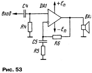
Further improvements come down to installing transistor current generators instead of resistors, voltage stabilizers in the power source, switching on emitter followers between individual stages - variations on this topic are endless, and those interested in UMZCH circuitry will study them for themselves, according to other publications. We will proceed to the calculation of the simplest circuit. The amplifier (Fig. 51) is nothing more than an operational amplifier (op-amp) in its simplest form. Op-amps have a number of advantages that ensured their universal and widest application. The input resistance and gain of an ideal op amp are infinite, the output resistance is zero. An ideal op-amp responds only to the voltage difference at its inputs. This means that a simultaneous (common-mode) voltage change at the inputs does not result in an output signal. Our op-amp is far from ideal: its input impedance is tens of kiloohms, its gain is several thousand, and the input signal common-mode suppression does not exceed 20...40 dB. Nevertheless, it turns on and works in the same way as an ideal op-amp (Fig. 53).
The input signal is fed through the decoupling capacitor C4 to the non-inverting input DA1 (what is in the triangle corresponds to the circuit in Fig. 51, but it can also be other op-amps with a powerful output, for example, K157UD1, K174UN11, etc.). Resistor R4 sets the zero potential at the input. Without negative feedback, which reduces gain and at the same time non-linear distortion, as well as expanding the band of amplified frequencies, the op-amp cannot work. OOS is fed from the output of the amplifier to the inverting input through the resistor R6. At direct current and lower frequencies, the C5R5 chain does not play any role, so the depth of the feedback is 100%. This means that the potentials at the output and at the inverting input are also zero. Indeed, the slightest deviation of the output potential, for example, in a positive direction, will be transferred to the inverting input through the resistor R6, amplified and will lead to a decrease in the output potential, compensating for the initial deviation. It is a different matter for 3H alternating current - the divider R6R5 operates in the OOS circuit, and only a part of the alternating output voltage equal to UvyxR5 / (R5 + R6) is transmitted to the inverting input. The voltages at the inputs are almost equal (let's not forget that the gain of the op amp is in the thousands), so the formula for the gain will be: K = Uvyx/UBX=1 + R6/R5. The reactance of the capacitor at the lower passband frequency of the amplifier fH must be less than the resistance of the resistor R5, so C5≥ 1/2πfHR5. To complete the calculation of the circuit elements in Fig. 53, it remains for us to choose the resistances of resistors R4 and R6. It is advisable to take them the same, then the same input currents of the op-amp, passing through these resistors, will also cause the same voltage drops. The voltage difference at the inputs will remain zero. Nevertheless, these voltage drops should not be large, it is reasonable to limit them to 50 ... 100 mV. Hence, R4 = R6 = (0,05...0,1 )/iin. For example, with iin = 1 μA, the resistances of the resistors are equal to 50 ... 100 kOhm. Let us now proceed to the calculation of the internal elements of the OS (see Fig. 51). The current of the input transistors VT1 and VT2 (it is the same) is i1 = i2 h21e where h21e is the static current transfer coefficient of the input transistors in a circuit with a common emitter (it should also be the same if possible). The total current of the transistors passes through the resistor R2, and the voltage drop across it should be 0,5 V (threshold voltage for opening transistors) less than the power supply voltage En. From here R2 = (En-0,5)/2i1 With h21e = 100 and iin = 1 μA, the current of each input transistor will be 0,1 mA, and the resistance of the resistor R2 at En = 6 V is 27 kOhm. Current i should create a voltage drop across resistor R1 sufficient to open transistor VT3, i.e. not less than 0,5 V. Therefore, the resistance of the resistor R1 should be R1 =0,5/i1 In our example, R1 = 5 kOhm. If you choose more of it, then a significant part of the current i will be directed to the base of the transistor of the final stage VT3. This can be allowed provided where i3 is the collector current of the transistor VT3; h21ЭЗ - its current transfer coefficient. The current i3 will be determined in the further calculation. Then you can proceed to the calculation of the pre-terminal and terminal stages, and it is better to start with the latter, since the mode of the former is largely determined by it. Here we need the collector characteristics of powerful output transistors, shown in Fig. 54 and given in reference books.
It is assumed that transistors VT4 and VT5 have the same characteristics, differing only in structure. Similar pairs of complementary transistors are produced by the industry (examples: KT315 and KT361, KT815 and KT814, KT819 and KT818 with different letter indices). The characteristics show the dependence of the collector current on the instantaneous voltage on the collector at various base currents. The dashed lines on the graph show the area of allowable modes of the collector circuit: from above it is limited by the maximum collector current, on the right - by the maximum allowable collector voltage, in the middle part - by the maximum allowable dissipation power of the transistor, calculated as the product of collector current and voltage. The load line must not cross the boundaries of permissible modes anywhere. As already mentioned, transistors VT4 and VT5 operate in a mode close to class B. This means that in the absence of a signal, the voltage across the transistor is equal to Ep, and the current is close to zero (the right side of the load line). On the positive half-wave of the signal, the upper transistor (VT4) opens in the circuit, on the negative half-wave, the lower one (VT5). Since the processes are completely symmetrical, consider the operation of the upper transistor. As it opens, the collector current increases, and the collector-emitter voltage drops, since a positive half-wave of voltage is released on the load - the BA1 head. Moving along the load straight line to the left and up, we determine ik max and Uk min shown in fig. 54. If there are no characteristics, then the current ik max is taken slightly less than the maximum allowable collector current, and Uk min means the saturation voltage of the collector-emitter (voltage drop across the transistor when it is fully open). Knowing the last two parameters allows you to calculate the power output by the amplifier. Indeed, the range (amplitude) of the AC voltage of the AF at the load will be En - Uk min, and the current amplitude - ik max. Power will be P \u2d (En - Uk min) ik max / XNUMX. In practice, it is often with this that they begin the calculation - having given the output power, they determine the supply voltage En and select the type of output transistors that provide the required maximum current and correspond in terms of maximum permissible parameters (Fig. 54). It should also be borne in mind that the collector voltage of a closed transistor can reach almost 2En - the maximum allowable value of the collector-emitter voltage of the selected transistors must be at least 2En. Knowing the current transfer coefficient (in large signal mode) of the output transistors h21e4 and h21e5 (again, it is desirable that they be the same), the maximum base current is found ib4 = ik max/h21e4 The collector current of the pre-terminal stage (recall that, unlike the output transistors, it operates in class A) must be significantly greater than ib4. Here, the shortcomings of the simplest scheme are revealed (see Fig. 51). The fact is that on the positive half-wave of the signal, the transistor VT3 opens and its increasing current opens the output transistor VT4. These processes are going well enough. But on the negative half-wave of the signal, the transistor VT5 should open, and its maximum base current is determined by the resistor R3, and the voltage across this resistor at the peak of the negative half-wave is even less than Uk min! That is why it is necessary to set a large collector current of the pre-terminal stage i3 10 ... .20 times more than ib4, and calculate the resistance of the resistor R3 according to the formula R3 = En/i3. Of course, this is unprofitable - you have to put a rather powerful transistor in the final stage, and the efficiency of the entire amplifier is reduced. The following measures correct the situation: increasing the current transfer coefficient of the output transistors (installing composite transistors, two or at least one in place of VT5), using a transistor current generator instead of the resistor R3, turning on the "voltage boost". In the latter case, the resistor R3 is made up of two resistors connected in series, and their midpoint is connected through a large capacitor to the output of the amplifier. The local positive feedback that has arisen contributes to a better opening of the VT5 transistor. The last part of the amplifier that has not been considered is capacitor C1, which corrects the frequency response in the higher frequency region. Its capacitance is usually small - tens of picofarads. It will be discussed in more detail in the next section. Question for self-test. Calculate UMZCH with the following parameters, input voltage - 0,1 V, supply voltage - ± 6,3 V, load resistance - 4 Ohm, frequency response - 50 Hz ... 12,5 kHz. Select the type of transistors. Determine the maximum output power on a sine wave. Response. Let's start with the last one - let's calculate the output stage in the maximum power output mode. Putting the residual voltage on the collector of the open output transistor Ukmin = 0,3 V, we obtain the amplitude of the variable component of the RF at the output Um = 6 V. Then the maximum value of the current through the transistor will be lm= Um/RH \u6d 4 V / 1,5 Ohm - \uXNUMXd XNUMX A. The output power on a sinusoidal signal will be P \uXNUMXd \uXNUMXd UmIm/2 = 4,5 W. The average value of the current of cosine pulses through the output transistors is 0,32lm (0,32 is the zero factor of pulse decomposition into harmonic components). So l0 = 0,32lm \u0,5d XNUMX A. Here we must add another quiescent current Ipok output transistors of the order of 0,05 A. Now we find the power consumed by the amplifier P0 = 2En(I0 + Ipok)= 7 W. As you can see, the efficiency of the amplifier in maximum power mode will be only R / R0 = 4,5 W / 7 W = 0,64 or 64%. At lower powers, the efficiency will be even lower. Each of the output transistors will dissipate power (P0 - P) / 2 \u1,25d 816 W. A good choice of transistors is a complementary pair of KT817, KTXNUMX (with any letter indices). Their parameters meet our conditions with a significant margin. The voltage gain of the pre-stages should be at least 6,3 V/0,1 V = 63. One transistor stage, given the load on the low input impedance of power transistors, will not provide such an amplification, therefore, at least two stages are needed. The diagrams in Fig. 51-53. The excess amplification is damped by the introduction of an OOS (Fig. 53) with a resistance ratio R6 / R5 of approximately 60 ... 70. Author: V.Polyakov, Moscow
Air trap for insects
01.05.2024 The threat of space debris to the Earth's magnetic field
01.05.2024 Solidification of bulk substances
30.04.2024
▪ Fully integrated opto-electronic four-channel multiplexer ▪ Internet speed doubled on the ISS ▪ The phone is charged from a cup of hot coffee
▪ site section Regulators of current, voltage, power. Article selection ▪ article Orientation and geographic projection. Fundamentals of safe life ▪ article Where was the guillotine invented? Detailed answer ▪ article Bookbinder. Job description ▪ article Universal matching device. Encyclopedia of radio electronics and electrical engineering
Home page | Library | Articles | Website map | Site Reviews
www.diagram.com.ua |


 Leave your comment on this article: