|
|


 Arabic
 Bengali
 Chinese
 English
 French
 German
 Hebrew
 Hindi
Hindi Italian
 Japanese
 Korean
 Malay
Malay Polish
 Portuguese
 Spanish
 Turkish
 Ukrainian
 Vietnamese
|
ENCYCLOPEDIA OF RADIO ELECTRONICS AND ELECTRICAL ENGINEERING Compact car amplifier. Encyclopedia of radio electronics and electrical engineering
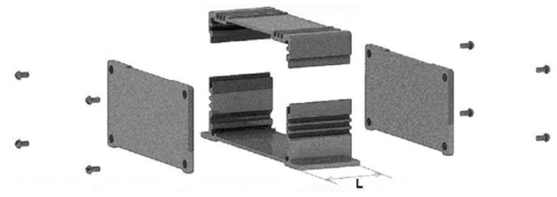
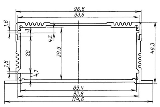
Encyclopedia of radio electronics and electrical engineering / Automobile. Electronic devices The article describes the design of a simple car stereo amplifier with a switching voltage converter. Its addition significantly increased the power of the amplifier on the popular TDA7293 or TDA7294 microcircuits - up to 78 W at a 4 ohm load, and the use of a ready-made case greatly simplified its manufacture. As often and rightly stated, the sound of a car's head unit can please only an inexperienced listener. In practice, it turns out that in most cases the real value of the output power of the PA radio does not exceed 20 W per channel with a load of 4 ohms, and when running on battery power drops to 16 watts. Actually, even with such power, any car interior can be sounded with high quality, if not for the peak factor of musical signals, which reaches 20 ... 25 dB in some compositions. So, the built-in PA of a car radio without limiting the dynamic range can deliver up to 5 watts per channel. Given the qualitative growth of the parameters of modern PAs, the issue of upgrading the playback path rests on the physical limitation of the dynamic range by the maximum output power of the built-in PAs, and the possibilities for its expansion have been exhausted by equipment manufacturers. Due to the high level of noise (including from outside) in the vehicle, the dynamic range is significantly reduced. The noise isolation of the body and the increase in the sound pressure level of the speakers help to increase the dynamic range of the listening. Installing an external PA at the initial stage of modernization is, in my opinion, the least labor-intensive. It should be noted that the refinement of the car audio system must begin with the installation of a better front speaker. Modern multimedia devices for cars are equipped with line outputs for connecting external amplifiers. The industry offers many high-quality automotive PAs, but their high cost is a significant constraint on upgrades. Connecting the PA to the outputs of the amplifier built into the radio, in my opinion, is not advisable. The proposed device has minimal functionality, but has a number of positive features: a powerful unstabilized power supply, a good amplifier, a minimal package size, and the absence of low-quality input active filter components. The nominal supply voltage is +/-25 V, which makes it possible to increase the power at a load of 4 ohms up to 78 watts. Unlike many designs described on the Internet, this two-channel PA is assembled in a standard, affordable and inexpensive Gainta aluminum case, shown in fig. 1. Width (size L in Fig. 1) - 100 mm. The dimensions of the main board are 93,6x96 mm, which allows it to be inserted into special slots in the case. The priority in the project is given to the compactness of the device, so surface-mounted parts are used.
The PA was designed for a specific CD player, for which the nominal load of the line output is 10 kOhm. The device consists of an unstabilized voltage converter (PN) and an PA based on two TDA7293 microcircuits (or TDA7294, taking into account differences in the pinout), as well as a control unit for an external signal Remote signal STBY amplifier. The amplifier circuit is shown in fig. 2. The converter with the soft start function is assembled on the TL494 chip and field effect transistors. The overall power of the transformer is about 300 W, and the use of two pairs of transistors in each leg of the converter allows you to deliver more power to the load. The calculation of the transformer and the choice of the magnetic circuit was carried out using the useful free program EXCELLENIT5000 [1]. There is an opinion that PAs with a pulsed PSU without stabilization provide better sound than with a stabilized PSU. Resistors (47 ohms) are included in the gate circuits of the power transistors of the converter, which narrows the spectrum of interference created by the inverter. On the smaller board there is a power-on control unit and a PN controller, on a larger board - PN and PA. The output circuits of the PV are not galvanically connected to the primary power source.
To turn on the PA, it is necessary to have a supply voltage of 12 V and a control voltage of more than 9 V at the input of the remote control. The voltage from the remote control input through the zener diode VD1 and the resistor R7 enters the base of the transistor VT2 and opens it. Capacitor C5 serves to delay turning on the PA and filtering noise at the input of remote control, resistor R8 provides the minimum current for the operation of the zener diode VD1. Transistor VT2 opens, and a voltage of about 0,7 V is set on its collector, the HL1 LED lights up and transistor VT1 opens, which supplies power to the DA1 chip and starts the PN. Resistor R5 is needed to support the closing voltage based on VT1 in the absence of a control signal, and R6 to limit the maximum current of the transistor VT2. In the presence of a secondary voltage PN, the voltage from the emitter VT1 through R1 is supplied to the radiating diode of the optocoupler U1, and it illuminates the phototransistor of the optocoupler. When voltage is applied to the DA1 microcircuit, a voltage of 14 V appears at its output (pin 5), which, through the capacitor C3, is fed to pin 4 of the TL494 pulse width control. As C3 charges, the voltage at pin 4 decreases due to the load resistor R2, and the pulse width at pins 9, 10 increases. This is how the soft start of the PN is organized. Resistor R2 is also needed to prevent the charging of capacitor C3 by the current flowing from the microcircuit (from 2 to 10 mA). The built-in error amplifiers in TL494 are not used, the non-inverting inputs 2, 15 DA1 are supplied with voltage ION equal to 5 V from pin 14, and the inverting inputs are connected to the common wire of the PN. Resistors R3, R4 and capacitor C4 set the switching frequency of the PN to about 50 kHz. The place for the resistor R4 is reserved on the board for possible correction of the frequency of the PN. Capacitors C2 and C1 block RF interference. From pins 9, 10 of DA1, field-effect transistor (FET) control signals through the XP / XS1 connector (ZL201-10G, ZL262-10SG manufactured by NINIGI) are fed to the main PA board to the FET gates On the elements R12, VD4, VT4 (R13, VD5, VT5 ) FET gate capacitance recharging circuits are assembled. Resistors R19-R22 reduce the FET switching speed and reduce switching noise. The PTs are connected in pairs to the primary winding of the transformer T1, to the midpoint of which the voltage of the vehicle's on-board network is supplied through the fuse-link FU1 and the U-shaped filter C6C7L1C10C13C14C18. Capacitors C10, C13, C14, C18 are connected in close proximity to the midpoint of winding I of transformer T1 to reduce interference. Diode VD2 serves as protection against reverse polarity of the supply. The alternating voltage from the secondary winding T1 is rectified by diode assemblies VD7, VD8, filtered by capacitors C20-C23 and then fed to the UMZCH microcircuits. In addition, the voltage of +24 V through the resistor R14 is supplied to the transistor of the optocoupler U1 and, if there is voltage at the input of the remote control device, it is supplied to the base of the transistor V73. Elements R9, VD3, VT3 are necessary to ensure the rapid discharge of capacitors in the STBY, MUTE circuits of the DA2, DA3 microcircuits after the remote control signal is lost. This is due to the fact that when the radio is turned off, significant voltage surges appear at its linear outputs, which lead to clicks in the speakers. In most home-made devices, STBY MUTE signals are generated through a limiting resistor connected to the positive power circuit, so when the radio is turned off, the PA does not go into STBY mode until the capacitors in the power circuit are discharged. In the same design, the PA turns off almost immediately after the disappearance of the remote control signal from the radio. To ensure the symmetry of the load on the IP and to be able to work in the bridge mode, one PA channel operates in the inverting mode. To minimize the interference introduced by the voltage drop on the "power" wires, the common wires of the signal and supply circuits are connected only in the low-current part through resistors R11, R15. Elements R16, C9, R23, C11, R27 and R32 (R17, C8, R18, C12, R24, R29 and R31, R33) form band limiting filters and set the channel gain. Since the inclusion of microcircuits DA2, DA3 is different, to equalize the gain in the channels, you can adjust the total resistance of the OOS resistors (R31 and R33). There is no place for the resistor R31 on the board; if necessary, it is installed on top of R33. In the simulation of microcircuits in the form of an op-amp in the Microcap 9 software package, the resistance of this resistor turned out to be 80 kOhm. The decline in the LF region (-3 dB at a frequency of 17 Hz) is due to the scope of the PA. First, front speakers, due to their size and acoustic design, greatly reduce efficiency at low frequencies; secondly, the resulting frequency response in the car interior usually has a rise in the low-frequency region by several decibels. The transformer is assembled on an Epcos 29,5x19x20 (B64290-L756-X87) toroidal magnetic core made of N87 material. The primary winding has 8 turns of wire with a diameter of 0,51 mm, folded into eight strands, with a tap from the middle. The initial data and calculation results are shown in Figs. 3. The secondary winding contains 18 turns of the same wire, folded into three strands, with a tap from the middle. The coils are evenly distributed around the perimeter of the ring. Choke L1 is wound on an annular magnetic circuit measuring 23x14x9,5 mm made of powdered iron T90-52 Micrometals and contains eight turns of PEV 0,51 wire, folded into eight cores. The inductance of the inductor may differ, it is only important to remember that overheating is over 75 оC for such a throttle is unacceptable.
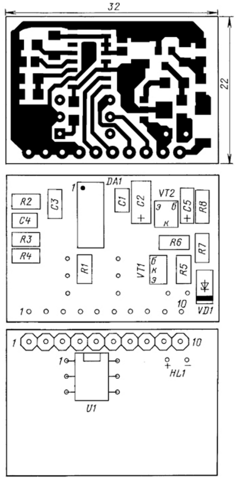
Assembly of the device should start with a smaller board (its drawing in Fig. 4 on a scale of 2: 1), in the diagram of Fig. 2 parts located on it are circled with a dash-dotted frame. After installing all the parts, a 1 V voltage source is connected to the contacts of the XP12 connector. +9 V must be applied to pin 12, and pins 1-4 connected to a common wire. Then close contacts 9 and 10, the LED should light up. A voltage of about 1 V will be established on the collector VT11, a voltage of 14 V will appear at pin 1 DA5, no more than 4 V at pin 0,5, and a meander with an amplitude of 9 V at pins 10, 11. In the absence of an oscilloscope, the presence of pulses at outputs 9 , 10 is defined by a digital multimeter as a constant voltage of 5 ... 6 V.
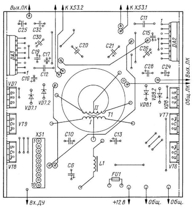
Then they assemble a large board (Fig. 5, 6), installing all the details, except for the PA chips DA2, DA3. It is also necessary to install wire (insulated) jumpers. It is desirable to solder the transistors at the same height, this will facilitate their fastening. Since the paired diodes in the TO-220 package with a common anode are scarce, the board provides places for their replacement with diodes in the DO-27 package.
After connecting the boards using the connector and supplying 12 V to the designated areas from the power supply and the remote control enable signal, voltages of +20 and -21 V should appear on capacitors C25 and C25, respectively, and on the VT3 emitter - about +8 V relative to the midpoint output winding of the transformer. In this case, the parts of the converter should not heat up, and the current consumption should not exceed 0,3 A. After checking the PN, the DA2, DA3 microcircuits are soldered. Unused microcircuit leads are shortened by 3 ... 4 mm. It is important to install the microcircuits strictly perpendicular to the board, otherwise they will not adhere to the case with the entire plane and may overheat. To reduce the effect of interference on the amplifier circuits, additional capacitors C26, C28 (C30, C32) with a capacity of 470 uF with low impedance (low ESR) were added near the power supply pins of the microcircuits. To reduce interference, the tracks from the power pins of the preliminary stage and the output stage of the TDA7293 are connected at the soldering points of the pins of these capacitors. Then wires are soldered into the board to connect external connectors. The power connector (terminal block DG58C-A-2P13 from Degson Electronics) requires at least 2 mm wire2. A segment 50 ... 70 mm long is soldered into the board. The cables connecting the board with RCA connectors (XS3.1, XS3.2) are soldered in the same way. To do this, use any soft cable. In the same way, solder the wires to the X4 output connector (terminal block DG58H-A-04P-13 from Degson Electronics). The cross section of the output wires must be at least 0,5 mm2. The soldering points of the wires must be strengthened with hot glue. For the remote control signal wire, a hole with a diameter of 2 mm was drilled in the side cover, through which a wire about 20 cm long was brought out. To fix it, it is advisable to tie a knot from inside the PA case. Next, the board is inserted into the groove of the case and the holes for the screws for fastening transistors and microcircuits are marked. The holes are made with a drill with a diameter of 3,6 mm, then they are countersunk for the installation of "sunk" screws. Powerful FETs, diodes and output microcircuits of the PA are attached to the case (photo in Fig. 7) with M3 screws through insulating mica spacers using insulating inserts for the screws. Gaskets for microcircuits must be smeared with thermal paste, for example, KPT-8.
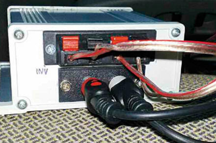
Then, X4 output connectors are installed on the plastic walls of the case and the corresponding wires from the printed circuit board are connected to them (photo in Fig. 8). After that, connect the signal cables to the connectors on the amplifier panel (photo in Fig. 9) and once again check the operation of the system as a whole; if everything is in order, it is advisable to glue the wires on the output connectors and the XP / S1 connector, overall capacitors and transformer with hot glue, as they will work in vibration conditions. Then the body is assembled completely.
Before installation in a car, it is desirable to run the amplifier for several tens of hours to check its reliability. Power connection directly in the car must be made with wires with a cross section of at least 2,5 mm2 as short as possible (Fig. 10). You need to connect them to the battery terminals through a 15 ... 20 A fuse, lead both wires to the amplifier from the positive and negative terminals. Often, due to poor-quality wiring in a car, in order to avoid interference, it is necessary to run wires from the battery and to the radio.
Due to the small size of the case (heat sink area of about 400 mm2) during operation, the PA heats up to 40...50 оC. This is the normal temperature for amplifying equipment, if air circulation is provided when installing the device in the cabin. In real use in a car, a significant improvement in the sound of the system and ease of placement can be noted. Even during long-term operation at maximum power for speakers Focal polyglass V1, the temperature of the PA case does not exceed 60 °C. Naturally, one should not expect miracles from such an amplifier, but it can definitely be argued that it will "replay" most of the crafts of the lower price range, while maintaining the characteristics of the TDA7293 microcircuits. Some parameters of the PA were checked using the Right Mark Audio Analyzer 6.0 (RMAA) computer program. At an output power of 15 W at a supply voltage of 12,6 V, harmonic distortion in the channels is 0,045 and 0,019%, and intermodulation distortion is 0,024 and 0,026%. The signal-to-noise ratio is about 90 dB. Contrary to the popular opinion on the Internet forums, the inverting inclusion of the microcircuit (in the right channel) showed the worst result in terms of the measured parameters. Using a typical circuit from the reference documentation for the microcircuit [2] turned out to be the best option. Possible replacements: the PN TL494 chip has analogues - YuA7500, MB3759, UPC494, IR3M02, KP1114EU4. Instead of IRF3205, you can install any modern field-effect n-channel transistors, for example, IRFZ44, IRF540, BUZ111S, STP80NF06, IRF1405 for a voltage of more than 50 V, and it is permissible to use only one pair of transistors. BC817 transistors can be replaced by 2N5550S, MMBT100, MMBT2222, 2SD1484, and BC807 transistor by 2STR2160, BCX17, MMBT591, PMBT2907. Transistor BCX51 replace BCX52, BCX53, 2SB1027, 2SB1313, SB1123U. If necessary, the selection of types of transistors can be carried out according to the reference book [3]. Two diode assemblies VD7, VD8, designed for a direct current of at least 3 A and a voltage of more than 80 V, can be replaced by four diodes FR302-FR304, UF5404, RGP25G. On fig. 11 shows the layout drawings of the front and rear panels of the PA unit for the elements and switching units used by the author.
Literature
Author: Yu. Ignatiev, Ivano-Frankivsk
Artificial leather for touch emulation
15.04.2024 Petgugu Global cat litter
15.04.2024 The attractiveness of caring men
14.04.2024
▪ Xiaomi Fire Extinguisher Bottle
▪ site section Color and music installations. Selection of articles ▪ Article Garden paths. Tips for the home master ▪ How do seeds propagate in nature? Detailed answer ▪ article Motor grader driver. Standard instruction on labor protection ▪ article Glyants-starch Lustrin. Simple recipes and tips ▪ article Economic stabilizers. Encyclopedia of radio electronics and electrical engineering
Home page | Library | Articles | Website map | Site Reviews
www.diagram.com.ua |


 Leave your comment on this article: