|
|


 Arabic
 Bengali
 Chinese
 English
 French
 German
 Hebrew
 Hindi
Hindi Italian
 Japanese
 Korean
 Malay
Malay Polish
 Portuguese
 Spanish
 Turkish
 Ukrainian
 Vietnamese
|
ENCYCLOPEDIA OF RADIO ELECTRONICS AND ELECTRICAL ENGINEERING EA class amplifier (Super A, Non switching). Encyclopedia of radio electronics and electrical engineering
Encyclopedia of radio electronics and electrical engineering / Transistor power amplifiers (Five options) A detailed description is given to study the principle of operation and manufacture. This audio power amplifier has been designed under the following conditions:
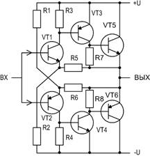
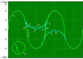
Principle of operation Initially, this UMZCH (Fig. 1) was developed as a model for studying nonlinear distortions in amplifiers. The input stages were not supposed to have "step" distortion at all. For this, cascades are most suitable, as it were, connected in parallel between + and - power supplies (VT1, VT2), for which they received the name "parallel". The emitter VT1(VT2) was connected to a potential below the negative input voltage in order to be able to control the moment and nature of closing VT5(VT6) (mode A, EA, AB, B). Then the idea arose to supply the emitters VT1, VT2 with a feedback voltage (OOS) through R5 (R6) to the already formed parallel (they are also composite) cascades, which lowers the potential of the emitter VT1 (VT2), preventing the abrupt closing and opening of VT5 (VT6 ), and thus form quiescent currents in the EA mode. The results of the research are summarized in an oscillogram of the output currents (Fig. 2), where (1) is the current in the load, +I is the current VT5, -I is the current VT6. The modes were set deliberately to determine the threshold for the appearance of distortions. Point 2 - "step" type distortions in mode B, when VT5 closed sharply, and VT6 has not yet opened. In point 2, signal bursts with a different frequency are possible, which are present in the signal composition or when two frequencies are simultaneously fed to the amplifier input. Such a PA has a high harmonic coefficient, the HF in it will sound sharp, with hissing overtones, and the sinusoid will have an increased slope of the decline-rise. The transistor, which was slowly opened on small signals, then opens sharply, distorting the signal. The correct trajectory is line 3. It can be seen that a sinusoid (period) has formed relative to line 3 (half-period), which means overtones with doubled frequency (boom). When mode B is improved, area 2 turns into a bright dot and then disappears. Further, when studying non-linear distortions, it became clear that waveform distortions and an increase in the harmonic coefficient (point 4) occur even in mode A with high quiescent currents, if the opposite arm closes disproportionately to the signal (too sharply), thereby accelerating the current increase in load. The sound of such a mind will be sonorous, with a metallic echo, like when hitting a rubber ball. For this reason, some amplifiers with high parameters and high quiescent currents sounded worse and had a worse natural sound than simpler amplifiers in terms of circuit design. In mode A, if the quiescent current is rigidly stabilized (in this case, 250 mA, dashed line), a sharp break occurs at point 5, which immediately affects the linearity of the characteristic of the lower arm (4) that opens at this moment. At point 4, breaks and bursts of the output signal are possible. This means that it is not so much the quiescent current of transistors that is important, but their smooth (as close as possible to the shape of a useful signal) opening and closing. This fully confirms the correctness of the source [1], and makes it possible to apply the economical mode A (EA) in this PA (Io, lines 7 and 8 in Fig. 2). This mode is also called Super A, or Non switching (without switching) [1], but the name EA is closer to the truth. The fact is that EA produces a dynamic reduction of quiescent currents without degrading the parameters (with improved sound quality!), which reduces the heating of the output transistors by reducing through currents, increases the efficiency and efficiency of the amplifier.
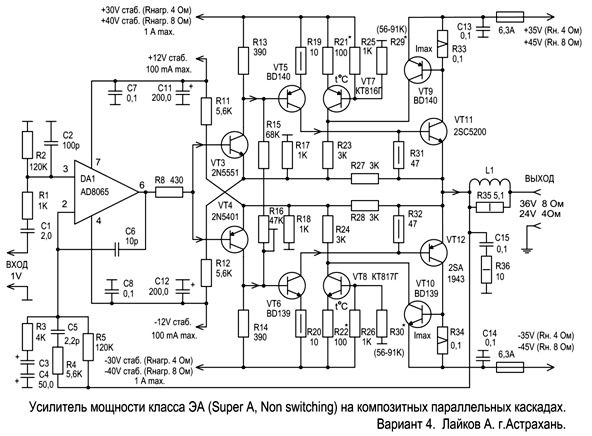
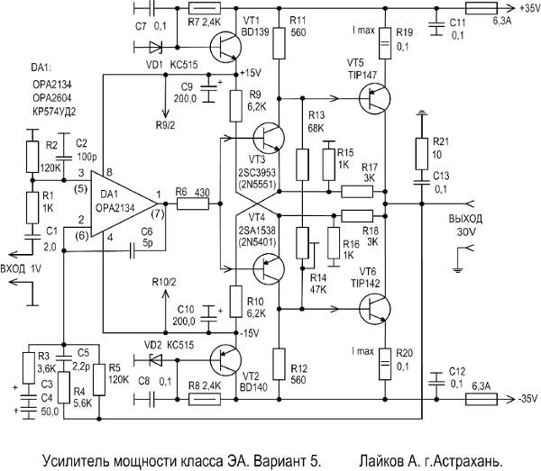
The principle of the amplifier (Fig. 3) The input signal is applied to the non-inverting input of the op-amp and amplified to 8V. From the output of the op-amp through R8, the signal is fed to the bases VT3, VT4. Since the emitters VT3 and VT4 are connected to a stabilized voltage source, and the power supply of the op-amp is also stabilized, the collector current VT3, VT4 depends only on the signal level, and depends little on the supply voltage. In fact, VT3(VT4) is a controlled current generator for VT5(VT6), which means that the influence of Upit on the collector current of VT5 will also be weakened. And the current VT11, in turn, depends on the collector current VT5. This means that in the amplifier there is no modulation of the useful signal by the supply voltage even without feedback, and the sound quality, especially at low frequencies, will be the same as in amplifiers with a stabilized power supply. Power drawdowns will be noticeable only at maximum power, with an output voltage close to the supply voltage. Transistors VT3 and VT5 (VT4 and VT6) make up composite cascades, into which a divider is introduced that determines the gain. Such a successful combination makes it possible to apply a negative feedback signal (NFB) directly to the VT3 (VT4) emitter circuit through R27 (R28), and at the same time allows you to easily form the operation of the output stages in the EA mode, obtaining high linearity at a high slew rate and gain . The OOS voltage is applied to the emitter VT3 (VT4), preventing its abrupt closing. Even when operating with current cutoff at maximum signal levels (osc.6), the output transistors open smoothly in advance and do not create distortion at low signal levels (the region most favorable for the occurrence of harmonics). The gain of the transistor part of the amplifier is equal to the ratio R27/R17 (R28/R18)+1. The gain of the entire amplifier is equal to the ratio R5/R3+1. The sensitivity of the amplifier is set by selecting R3. Selecting the amplifier operating mode When developing and testing any UMZCH, the main task is to achieve maximum quality with minimal heating. The amplifier was tested in all modes from A to B (Fig. 2, oscillators 6, 7, 8). In this PA, there is actually no mode B. The cutoff of the upper-side current (line 6) occurs at a lower-side current of more than 2A, which has little effect on the shape of the useful signal, and is actually an AB mode, only with the formation of a decline-rise according to the EA principle. It should be noted that the shape of the quiescent currents along osc.7 is idealized and practically is mode A. Unreasonably low efficiency, heating differed little from mode A, while there is no noticeable improvement in sound. And even vice versa, (according to the author) the sound was too smoothed out, the treble was lost on some compositions. In terms of economy, the most ideal is the osc.9 mode, with the quiescent current dropping to 0 at the maximum signal. The current shape was experimentally determined at maximum efficiency (osc. 8, 40 mA, without cutoff), and the first version of the amplifier was made. Then, by increasing the local OOS, it became possible to increase the dynamic increase in the current of the input transistors, which reduced the harmonics by half. The sound quality has improved. At the same time, it turned out that when the EA mode brings the current to a straight section, there is no longer a difference whether there is a current cutoff or not (oscillators 6 and 8). The sound hardly changes. This is how the second and following options were made. Of course, anyone can choose any of the family of quiescent current characteristics (Fig. 2) at their discretion. To increase the residual current (operation without cutoff), it is necessary to reduce R13-R14 to 360 ... 340 Ohm, increasing the constant component using R16. In order to give the quiescent current the form osc.7, it is necessary to reduce R11-R12 to 5,6 ... 5,1k. (Changes must be made with the output transistors disabled.) The first version of the amplifier Its scheme is completely identical to that shown in Fig. 3, and differs from the following ones only in the ratings R13-R14=360 Ohm, R27-R28=4,3k. The quiescent current has the form osc.8. The second version of the amplifier (Fig. 3) differs from the first one by changing the operating modes of VT3-VT4 and introducing a deeper EA mode (meaning a smoother rise-fall of the quiescent current). The dynamic current increase on R13-R14 has been increased and its constant component has been reduced (R15-R16). In addition to improving the sound quality, this increased the efficiency of thermal compensation. The deeper EA mode significantly reduced the level of voiced timbres (odd harmonics), and almost completely eliminated any timbre coloring of the sound. In combination with the zero output impedance of the amplifier, this makes any speakers sound very high quality. With the right choice of op amp, selection of transistors by gain and element ratings for shoulder symmetry, the harmonic coefficient is no more than 0,0006% at 1 kHz, and 0,002 at a frequency of 20 kHz. The rest current has the form osc.6 (0…5 mA). The third version of the amplifier (Fig. 4) Ways to further improve the parameters follow from the features of the element base. It is known that op amp distortion increases with frequency, output voltage, and current. It is difficult to achieve all the high parameters in one OS. The way out of this situation is to use a buffer stage from an op-amp with a high load capacity, i.e. composite inclusion of two op-amps. The output voltage of the first op amp is immediately reduced by 2-4 times, the harmonic coefficient is almost the same, and the gain of the second (buffer) op amp is doubled. As the first stage, it is best to use an op-amp with field-effect transistors at the input, with a very low Kg and the first pole above the audio range, and as the second - an op-amp with TOC, which have a very high output voltage slew rate and load capacity. High frequency TOC op amps have very low distortion in the audio range. It is also known that the gain and linearity of the characteristics of the transistor depends on the collector current, i.e. the smaller the current range, the lower the distortion. The output is the use of paired transistors in the output stages. Based on this, a third version of the amplifier was developed. With the correct selection of the op-amp, transistor gains and element ratings for shoulder symmetry, it is realistic to achieve a harmonic coefficient of no more than 0,0005% per 1 kHz, and no more than 0,001 in the entire frequency and power range.
Fourth amplifier option Its difference is in the use of a stabilized power supply for the pre-terminal stages, the use of FF op amps, and the ability to assemble a printed circuit board on SMD components (surface mount), which significantly reduces its dimensions. It is necessary to select SMD analogues of the transistors indicated in the diagram. As noted above, the sound quality and output voltage level of this amplifier do not depend on drawdowns and ripples in the supply voltage. The use of a stabilized power supply for the pre-terminal stages in this case only gives the independence of the quiescent current of the output transistors from large changes in the mains voltage, and can be applied at the request of the manufacturer. The numbering of components is left according to options 1 and 2.
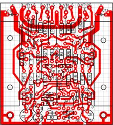
Fifth amplifier option The use of composite transistors in the final stages made it possible to simplify the circuit and amplifier settings, which is important for beginners and inexperienced radio amateurs. A significant reduction in its dimensions allows it to compete in dimensions with the integrated UMZCH, having higher parameters. At the same time, the gain linearity at low frequencies is greater than that of UMZCH microcircuits, the output voltage is greater at a relatively low supply voltage, and insensitivity to supply voltage drawdowns, which is especially important for small-sized power supplies. The diagram of the two-channel version is shown in the figure below. In this case, the OU and voltage regulators VT1-VT2 are common.
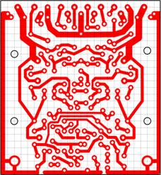
Amplifier option 5 requires little to no adjustment. It all comes down to checking the supply voltages, the absence of a constant voltage at the output, and setting the desired quiescent current with the maximum heated output transistors. The drift of the quiescent current with temperature is less here than in option 2 due to the lower current gain, but due to the large voltage gain of the composite transistors, excessive amplification and clipping of the signal is possible, which is not always useful for speakers. Therefore, R19-R20 should not be made less than 0,075 ohms, even for powerful speakers. If desired, you can add thermal control and current protection from option 2. If you have difficulty measuring the resistance of 0,075 ohms, then you can get out of the situation in two ways. 1) Connect two 0,15 ohm resistors or four 0,3 ohm resistors in parallel. 2) Measure the resistance of a constantan or nichrome wire (for example, by disassembling a 0,51 Ohm, 1% wire resistor), straighten it, and accurately divide it into equal parts along the length, obtaining the desired resistance. It is advisable to tin the ends of the segment on an aspirin tablet and wipe it with alcohol. A straightened piece of nichrome will not have inductance, and can be soldered to the board in the form of a jumper or bracket. The harmonic coefficient of the amplifier of the 5th option was not measured, but subjectively in terms of sound it is no more than 0,008% in the entire frequency and power range. As an example, in fig. 12-13 shows the printed circuit board of the two-channel version of the amplifier. The output transistors are TIP142T/TIP147T in TO-220 cases, and having smaller dimensions than TIP142/TIP147 in TO-3R cases. When embedded in multimedia speakers where there is vibration, R13-R14 are replaced by one constant 92 ... 100k. In a miniature version, on small radiators, it should be selected such that the quiescent current on cold radiators is 5 ... 10 mA, and when warmed up it never rises above 40 ... 60 mA. This mode can be classified as AV + EA. Capacitor C1 - small-sized ceramic, C3 - non-polar electrolytic. Amplifier parameters completely dependent on the type of OS used. The maximum possible sinusoidal output power of the amplifier of the second option is 120 W, but at a load of 4 ohms and a supply voltage above +/-35V, you need to limit the current of VT11, VT12 (R33, R34) or power them up, otherwise the power dissipation on the output transistors will exceed the maximum allowable. When applying a load of only 4 ohms, the supply voltage does not need to be raised above +/-35V. True, this will reduce the output power at a load of 8 ohms. According to the author, speakers with a resistance of 6-8 ohms have a more natural sound, and speakers with 4 ohms have more power output and dynamics. The frequency response of the amplifier is linear from direct current (without C1) to 200 kHz (without C2, C6), with a smooth decrease in amplitude from 200 kHz to 1 MHz. When a signal with a frequency of 1 MHz with amplitude modulation with a frequency of 1 kHz was applied to the input of the amplifier, it was received by a medium-wave receiver. A constant voltage was applied to the PA input (without C1) from 0 to 1V in 10mV steps, while the output voltage increased absolutely linearly from 0 to 30V, i.e. The amplifier behaved like a precision DC amplifier, which indicates its high gain linearity and, as a result, low harmonics and high sound fidelity. The amplifier was tested with rectangular pulses with a frequency of 2 kHz at a resistive load of 6 ohms. In this case, an output voltage slew rate of 30 V/μs was obtained and was limited only by the source of rectangular pulses; no distortion of the signal shape and no spikes were observed. Rated output voltage = Upit.-5 V. Maximum output voltage of the amplifier = Upit.-3V. When the supply voltage is reduced by a bipolar regulated power supply, the amplitude of the output signal does not decrease until the power supply reaches the value Uout + 5V, and when Upit = Uout + 3V, the output signal is gradually limited. The output impedance of the amplifier = 0. The amplifier is not sensitive to the background of the power supply with a variable component up to 100mV. Supply voltage range - from +/- 25 to +/-40V. Distortions were measured using two G3-118 generators and notch filters included in the set. The level of total non-linear distortion, when signals from 20 Hz to 20 kHz were applied to the input, was lower than given in [1] (Fig. 8), and was at the level of interference of the S1-65A oscilloscope itself (0,2 ... 0,3 mV at an output voltage of 32V), which implies a harmonic coefficient of no more than 0,002%. The same was shown by measurements with a computer spectrum analyzer. But at the same time, the main goal was to fulfill condition 2. The amplifier was tested and operated at Io = 150 mA with a high-quality heatsink. Despite the relatively large number of parts, the amplifier itself consists of a microcircuit and 6 transistors (VT3, VT4, VT5, VT6, VT11, VT12). VT1 and VT2 - voltage stabilizers +/- 15 V; VT7, VT8 - nodes for thermal compensation of the quiescent current of the output transistors; VT9, VT10 - maximum current limiters (6A). VT1, VT2, VT9, VT10, VD1, VD2, R9, R10, R19-R20, R33, R34 in the presence of a separate stabilized +/- 15 V source and with a decrease in output power (Upit. = +/-25V, Pout 50W) from the scheme, you can exclude and make a simplified small-sized version of the PA. Temperature compensation device It should be noted that the quiescent current of the amplifier can change significantly when the transistors (especially VT3-VT4) warm up and the supply voltage changes, so you need to accurately select the operating point of the VT7-VT8 transistors (compensators for changing the quiescent current from temperature and supply voltage). At the same time, local fluctuations of the quiescent current within +/- 20 mA do not affect the parameters of the amplifier. After the studies of the thermal modes of the UMZCH, the author came to the following conclusions: 1. An increase in the quiescent current of the output transistors by 2-3 times can occur even with a slight heating of the lowest-power input transistor, therefore it is desirable to control the modes of as many stages as possible. 2. It is desirable to place each output transistor on a separate radiator without insulating gaskets and control its temperature. The temperature compensation device works as follows. Transistor VT7, a current generator, is mounted on a VT11 radiator through a mica gasket. (VT8 on VT12 radiator). When the radiator heats up, the current VT7 increases and is fed through R23 (R24) to the emitter circuit VT3 (VT4), covering it. The signal for limiting the current of the output transistors is also supplied here. By selecting resistors R21-R22, you can set different temperature conditions for the amplifier. In mode 1, a solid line (when R21, R22 = 100 ohms) the quiescent current will be stable up to 65-70 degrees, and then it will sharply decrease to 0. In mode 2 (R21, R22 = 68 ohms), the quiescent current decreases in proportion to temperature , i.e. the device maintains the set temperature. In mode 3 (R21,R22 = 150 ohms), the quiescent current will not increase with increasing temperature, but it will not decrease to reduce the heating of transistors (the device can withstand a given current). When changing the amplifier supply voltage from +/-25 to +/- 40V, it is necessary to select the value of R29-R30 so that the offset on R25-R26 is 0,41-0,432 V. The value of R29-R30 is calculated by the formula: R29 (R30) , kOhm = Upit. /0,432 - 1k. When the output transistors were deliberately reinstalled on radiators of a smaller area, the thermal compensation device rebuilt and maintained the specified thermal conditions. In combination with low sensitivity to power drawdowns, this makes it possible to integrate this PA into existing equipment, where there is not enough power of the power transformer (for example, "Vega 50U-122S"), or the area of \uXNUMXb\uXNUMXbradiators (music center). Of course, it is possible to assemble ultrasonic frequencies on microcircuits, but (according to the author) they do not have the same sound quality as PAs on discrete elements. Details and construction In the amplifier, it is best to use an op amp with a slew rate of at least 50 V / μs with a low level of harmonics and intrinsic noise, with field-effect transistors at the input. Transistors VT3, VT4 should be selected with the highest possible gain, low noise level and a weak dependence of the collector current on temperature. As VT5-VT6, it is desirable to use transistors with a high gain frequency and low collector capacitance. In the amplifier, it is quite possible to use the domestic op-amp KR574UD1 and transistors with gains of 130 - 150 in order to be able to remake an existing amplifier (for example, Amphiton) from the same parts. The maximum allowable voltage of all transistors in this case must be at least 80V. Depending on the required Uout, it is necessary to change the resistance R5, observing the condition: (R5/R3)+1=Uout/Uin. When using other output transistors (field-effect or when connected in parallel), you may have to select the resistance R31-R32 according to the voltage drop of 0,55V on them in the middle position of the R16 engine with VT11-VT12 turned off. According to the author's calculations, on the basis of this circuit, it is possible to design an PA with an output voltage of 80-100 V. (The amplifier is capable of producing an output voltage close to the supply voltage). Complementary pairs (VT3 - VT4, VT5 - VT6, etc.) of opposite arms should not differ in gain by more than 5%. Symmetrically located resistors of the upper and lower arms are also selected with a tolerance of 5%. This is a necessary condition for the symmetry of the output signal and the avoidance of non-linear distortion. Resistors R33 - R34 consist of two 0,2 ohm 2W resistors connected in parallel, located one above the other. R33, R34 must be used non-inductive. Do not use wire wound resistors. Coil L1 is wound on a resistor R35, contains 2 layers of PEL 0,8 wire and is impregnated with varnish or glue. L1, C9, R36 are mounted on the output board. The surface area of radiators VT5 - VT6 is at least 30 cm, VT1 - VT2 -1..2 cm. If you need to change the size of the board, it can be moved along the grid. All tracks are soldered. The current-carrying tracks of the power circuits and the loads are tinned with a thick layer of solder with a laying of one strand of copper wire. For all transistors mounted on radiators, the use of heat-conducting paste is mandatory, and for transistors of thermal sensors, gaskets must be made of mica. As C1 and C3-C4, it is best to use a non-polar electrolytic capacitor.
Option 5 Dual Amplifier Board
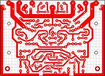
View from the soldering side. Size 55x60mm. The second and third variants of the amplifier can be assembled on a universal board (Fig. 8, Fig. 9). In the case of balancing the op-amp between pins 1-8 or 1-5, a jumper is placed at point X on pin 8 or 5. It must be reliable in order to avoid a gross imbalance of the op-amp. Resistor R6 can be switched to points + and - 15V on the board, or put a jumper, depending on the type of op-amp. If op amp DA2 is not used, the track should be cut at point X2. When using two op-amps, the resistor R8 switches to pin 6 of DA2. Setting up the amplifier After checking the correct installation, you should:
AC protection unit In emergency situations, when direct current flows through the speaker, its coil burns out, so the use of speaker protection is a prerequisite for powerful amplifiers. The protection unit (Fig. 10) works as follows.
Supply voltage range:..........+/-20…+/-60V
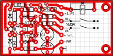
When the power is turned on, the capacitor C3 starts charging (from the power source through R7-R8). After 1 sec. the voltage on it reaches a value sufficient to open VT3, then VT4 opens, and the relay connects the speakers to the amplifier with its contacts. During normal operation of the PA, the alternating voltage from its output does not have time to charge C1-C2, and in an emergency, the constant voltage from the amplifier output will open VT1 or VT2 (depending on polarity), the voltage at C3 will decrease and the relay will turn off the AC. In case of false alarms of protection at high volume, the capacitance C1-C2 should be increased. A drawing of the printed circuit board of the AC protection unit is shown in fig. 11 and 12. It is advisable to use a separate speaker protection unit for each channel. The relay (U P1) must be powered from a source that has a lower power filter capacitance than the amplifier itself, so that when the power is turned off, relay P1 is turned off first. The relay should be used with the largest possible contact area and spring force, because miniature relays (especially reed relays) have cases of burning contacts and the inability to turn off in an emergency.
Literature 1. Yu. Mitrofanov. EA in UMZCH. Radio No. 5,1986, XNUMX
Author: Laikov A.V. (alexandr.laykov@rambler.ru); Publication: cxem.net
Machine for thinning flowers in gardens
02.05.2024 Advanced Infrared Microscope
02.05.2024 Air trap for insects
01.05.2024
▪ Improving the energy efficiency of existing wind farms ▪ Evaporation chambers in smartphone cooling systems ▪ Monitor Acer Nitro EI322QURP
▪ section of the site Mobile communications. Article selection ▪ Article Hospital Pediatrics. Crib ▪ article Where and when did people take shelter from the weather in armadillo shells? Detailed answer ▪ article Camellia eugenolus. Legends, cultivation, methods of application ▪ article Biogas on the farm. Encyclopedia of radio electronics and electrical engineering
Comments on the article: Vyacheslav What is the power and harmonic content of the amplifier option 5
Home page | Library | Articles | Website map | Site Reviews
www.diagram.com.ua |


 Leave your comment on this article: