|
|


 Arabic
 Bengali
 Chinese
 English
 French
 German
 Hebrew
 Hindi
Hindi Italian
 Japanese
 Korean
 Malay
Malay Polish
 Portuguese
 Spanish
 Turkish
 Ukrainian
 Vietnamese
|
ENCYCLOPEDIA OF RADIO ELECTRONICS AND ELECTRICAL ENGINEERING Transceiver YES-93. Encyclopedia of radio electronics and electrical engineering
Encyclopedia of radio electronics and electrical engineering / Civil radio communications The high parameters declared by the author of this transceiver may be taken with skepticism by some readers. However, the circuitry of the transceiver gives reason to hope that those who will repeat it will be able to get a device with very good parameters. At one time, a test during full-time KB competitions of a dozen and a half of the same type of UW3DI type transceivers, made by different radio amateurs, showed that their spread in dynamics reaches as much as 30 dB. So in the end, a lot depends on the experience of the radio amateur and his capabilities. The transceiver offered to the attention of readers is designed for telegraph and telephone communications with single-sideband modulation and amateur bands 1,9; 3,5; 7, 14, 21 and 28 MHz. During its development, the task was to create a modern device with high technical characteristics and at the same time relatively simple in terms of circuitry and allowing the use of widely used radio components. The best, but according to the author, amateur radio developments were used together with original circuit solutions. The result is a device with the following technical characteristics:
Some of the specifications, such as sensitivity, dynamic range, may seem exaggerated, but they really are. For measurements, we used a noise generator on a 2DZB lamp (1, 2] and the "Dynamics" device [1]. The latter was modified to reduce the spectral density of side noise and eliminate the penetration of the output signal bypassing the attenuator. The transceiver is made on a circuit with two frequency conversions. The choice of intermediate frequencies (5 MHz and 500 kHz) is dictated by the requirement for simplicity in the implementation of selective nodes, which at the same time provide a sufficiently high real selectivity. The receiving and transmitting paths are combined. The common ones are bandpass filters (BPF), a smooth range generator (GPA), mixers, quartz and electromechanical filters, and a block of reference frequency generators. The circuit diagram of the transceiver is shown in 1 drawing, diagrams of its individual nodes - in fig. 2 - 16. In the receive mode, the signal from the antenna input (jack XW1) through the attenuator A1 (see figure 2) and three-loop PDF Z2 (picture 3) with a gain of 6 dB enters the first mixer U1 (picture 4)made on transistors U1-VT1, U1-VT7, U1-VT8 [4]. Such a mixer has a low noise level, a relatively high transmission coefficient and suppresses the local oscillator signal at the output by about 60 dB. The inductor U1-L5, which has a large resistance at operating frequencies, is included in the source circuit of the transistor U1-VT1 and creates a deep negative feedback. For alternating current, it is shunted by the channel resistance of the transistor U1-VT7 (VT8). The local oscillator voltage supplied to the first gates of these transistors causes a modulation of the feedback depth, that is, it changes the slope of the transfer characteristic without shifting the operating point of the transistor U1-VT1. As keys in all mixers of the transceiver, KP350A transistors are used, which have good linear switching characteristics, and also allow introducing AGC through the second gates, which does not worsen the dynamic characteristics of the receiving part. The mixer gain is about 1. The intermodulation dynamic range - at the level of 90...95 dB - is achieved with the overall tuning of the transceiver The level of 100 dB or more is achievable only by very careful tuning of the U1-L1C6C7 and U2-L1C2 circuits (see figure 5), and without the use of ferrite interlineators, as well as a careful selection of the elements of the U1-R5VD1C1R3 circuit, which apparently provides "balancing" of the mixer. GPA G1 (see figure 6) made on transistors G1-VT1, G1-VT2 and U1-VT5, U1-VT6 and generates oscillations in the frequency ranges indicated in Table. one. Table 1
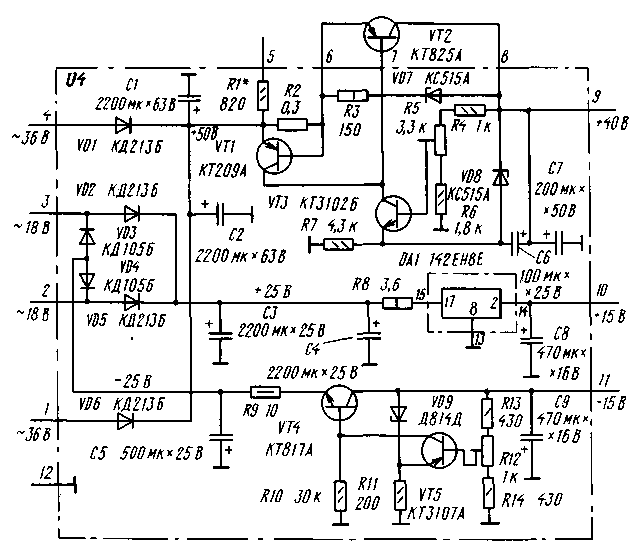
In order to simplify this node, only four relays were used for switching ranges, which naturally led to non-optimal stretching of some ranges. For normal operation of the mixer, the GPA frequency in the 21 and 28 MHz bands must be twice as high. This problem is solved by turning on the second transistor (L11-VT7) in the specified ranges, due to which the mixer switches twice as often, which is equivalent to doubling the GPA frequency. More details about this can be found in [5]. To ensure the highest possible mixer gain in the 21 and 28 MHz bands, the GPA has a system for rigid stabilization of the output voltage amplitude (G1-VD4 and U1-VT5), and it is also possible to smoothly change the bias voltage of transistors L11-VT7, U1-VT8 using trimmer resistor U1-R29. From the output of the mixer on the transistor U1-VT1, the voltage of the first IF (5 MHz) through the matching P-circuit U1-C6L1C7 goes to the amplifier, made on the transistor U1-VT2, is amplified by about 6 dB and is released on the circuit U2-L1C2, connected to crystal filter inlet U2-Z01 - U2-Z04 (picture 5) with a transfer coefficient of about 4 dB (due to the transformation of resistances). From the output of the quartz filter, the signal of the first IF goes to the second mixer, assembled on transistors U2-VT1, U2-VT3 and similar in principle to the mixer on transistors U1-VT1, U1-VT7, U1-VT8. The transmission coefficient of this mixer is -15...20 dB. The reference signal with an amplitude of 5 ... 7 V and a frequency of 4,5 MHz is fed to the second mixer from generator block G2 (Fig. 7), made on microcircuits G2-DD1 - G2-DD3 and transistors G2-VT1, G2-VT2 and generating oscillations with a frequency of 4,5 MHz and 500 kHz. The latter are obtained by dividing the frequency of the master oscillator on the IC DD1 (13,5 MHz) first by 3 (G2-DD2), and then by another 9 (G2-DD3). Cascades on transistors G2-VT1 and G2-VT2 are resonant amplifiers that generate signals of a good sinusoidal shape. The collector circuits of these transistors include diodes G2-VD1, G2-VD2, which make it possible to obtain signals with an amplitude of 40 ... 50 V on the circuits. Due to this, it was possible to use capacitive dividers G2-C7C8 and G2-C9C10 with a large division ratio allowed, together with the output filters G2-L4C11 and G2-L6C18C19L7C11, to obtain exemplary signals of the required amplitude and quality. The second IF signal (500 kHz) passes, attenuated by 6 dB, through the electromechanical filter (EMF) U3-Z1 (picture 8) and enters the input of a cascode amplifier made on transistors U3-VT2, U3-VT3. The amplifier is distinguished by a low level of its own noise and provides (from the EMF input) signal amplification by 60 dB. The second gates of the transistors of both the second mixer and the amplifier of the second IF are supplied with AGC voltage from block A5. The U3-VD1R4R3C11VT1 circuit provides a self-listening mode during transmission and eliminates switching clicks. From the output of the second IF amplifier, the signal is fed to the single-sideband signal detector, assembled on transistors U3-VT4, U3-VT5. It differs from the known ones by a large transmission coefficient (about 10 dB), low noise and background levels, as well as a large overload capacity. The reference signal with a frequency of 500 kHz comes from the block G2. From the output of the detector, the signal is fed to the inputs of the AGC node A5 (picture 9) and AF amplifier A6 (picture 10). When telegraph signals are received, the CW A6-Z1 filter with a bandwidth of about 300 Hz is turned on in the AF path, made on the op-amp DA2, DA3 according to the scheme given in [6]. At the request of the operator, a low-frequency phase shifter A6-L1R12C14C15 can be included in the path (mode conventionally called "Stereo"). The latter shifts the phase of the signal by 90° at a frequency of 900 Hz, which improves the real selectivity due to the selective properties of the human ear and, at a minimum, reduces operator fatigue, especially in CW mode. The applied correction and the selected gain (about 30 dB) of the A6-DA1 microcircuit made it possible to obtain a pleasant "transparent" sound of the signal. From the output of the detector (U3), a signal containing low-frequency and high-frequency (500 kHz) components enters the input of the emitter follower A5-VT1 of the AGC system, after which it branches into two channels. The low-frequency channel (A5-VT2, A5-VT3), which contains a logarithmic amplifier (A5-VT3), ensures the operation of the AGC and S-meter from 3 to 7 points of the S scale. The absence of a reference frequency of 500 kHz at the output of the voltage detector made it possible to use the signal FC for the operation of the high-speed channel A5-VD1VD2VT6. The cascade on transistors A5-VT6, A5-VT7 is two combined integrators with time-setting capacitors A5-C11, A5-C12. The introduction of the transistor A5 VT6 made it possible to significantly increase the input impedance of the integrator, and consequently, to reduce the capacitance of the capacitor A5-C12, which, in turn, allowed it to charge quickly. With the appearance of a signal for the first period of the IF voltage, the capacitor A5-C12 is charged, and the voltage on the collectors of transistors A5-VT6, A5-VT7 drops abruptly, which corresponds to a decrease in the AGC voltage and, consequently, a decrease in the overall gain of the receiving path. With the advent of the AF signal (much later), the transistor A5-VT4 closes, increasing the time constant of the AGC circuit, so that the overall gain of the receiver between the individual speech sounds is maintained constant (7). If the AF signal disappears for more than 100 ms, the transistor A5-VT4 opens, and the capacitor A5-C12 quickly discharges, restoring the sensitivity of the receiver in a short time, almost imperceptible to the operator. The high-speed channel ensures normal operation of the AGC with input signals up to S9 + 80 dB. In order to attenuate impulse noise, instead of the capacitor A5-C7, using the relay A5-K2, A5-C8 is switched on, as a result of which the AGC recovery time is reduced. Transistor A5-VT5 disables AGC in transmission mode. In general, the described AGC system has the following characteristics: the charging time constant of the AGC circuit with an abrupt change in the input signal is not more than 0,2 ms, the discharge time constant is not less than 25 s, the recovery time of the receiver sensitivity when the AF signal is lost is not more than 100 ms, without the oscillatory nature of the process of establishment and with a small aftereffect of impulse noise. In the transmission mode, the original signal is formed in block A4 (see figure 11), containing an A4-DA1 op-amp microphone amplifier, a balanced modulator (A4-VD2, A4-VD3, A4-T1), a DSB amplifier (A4-VT1) and a keyed telegraph oscillator (A4-VT2). The microphone amplifier has an input impedance equal to the signal source impedance, which helps to reduce high- and low-frequency interference. Amplified to a level of 3 ... 5 V, the AF signal is fed to a balanced modulator made on varicaps A4-VD2, A4-VD3. Such a modulator is characterized by very low non-linear distortion, large allowable input and output signal levels, as well as the ease of achieving large carrier suppression. The generated two-band signal is amplified by the transistor A4-VT1 and fed to the EMF A4-Z1, where the lower sideband is filtered out. The single-sideband signal is mixed in the mixer with a 4,5 MHz voltage coming from the G2 block. The total signal with a frequency of 5 MHz and an amplitude of about 7 V is supplied to the U2-L3C6 circuit, where it is limited by the diodes U2-VD1, U2-VD2 at a level of about 0,7 V, which compresses the dynamic range of the SSB signal to 20 dB. The crystal filter U2-Z01 - U2-ZQ4 gives the signal the necessary purity and quality after the specified limitation. From the filter output (more precisely, from part of the U2-L1C2 circuit), the filtered signal enters the second mixer of the transmission path (U1-VT3, U1-VT4, U1-VT7, U1-VT8), where it is mixed with the GPA signal G1. The cascade on transistors U1-VT3, U1-VT4 has a large stable gain (about 40 dB) and at the same time does not degrade the dynamic range of the receiving path (in the receive mode). From the mixer output, the signal enters one of the PDF circuits (Z2). The filtered signal is amplified by a broadband amplifier based on transistors A2-VT1, A2-VT2 (see figure 12) from 100 mV to the level of 7 ... 10 V, after which it enters the input of the power amplifier (PA) A3 (picture 13), where it is amplified in power up to 25 W at a load with a resistance of 50 ohms. After passing the band filter MIND Z1 (picture 14), this signal enters the attenuator A1 (picture 2), and from it to the antenna. The protection circuits of the powerful A3-VT1 transistor provided in the PA allow not only switching ranges in transmission mode, but also preventing its failure in other extreme situations. The transfer of the transceiver from the transmit mode to the receive mode, and vice versa, is carried out using the transistor switches of the switch S1 (picture 15)controlled by the contacts of a switch mounted in the pedal. Transceiver Power Supply U4 (See Figure 16) contains a network transformer T1, three full-wave rectifiers (U4-VD1, U4-VD6; U4-VD2, U4-VD5: U4-VD3, U4-VD4), a +40 V voltage regulator on a transistor U4-VT1 - U4-VT3 and stabilizers voltages + 15 and -15 V (the first - on the U4-DA1 IC, the second - on the U4-VT4, U4-VT5 transistors). All stabilizers are protected against current overloads and short circuits in the load. The design of the transceiver is block. Details of nodes Z2, U1 - U3, G2 are mounted on printed circuit boards made of double-sided foil fiberglass (see Fig. 17 - 21). the foil on the part installation side is used as a common screen wire. Around the holes for the leads of parts that are not to be connected to a common wire, it is removed by countersinking with a drill about twice as large in diameter. The remaining nodes are mounted on boards made of one-sided foil fiberglass (see Fig. 22 - 31). Figure 17
For PA filters (Z1), it is necessary to make two boards (they are installed one above the other on the transceiver chassis; in brackets in Fig. 31, the positional designations of the elements installed on the second board are indicated). When repeating the design, it should be taken into account that the contours of the printed conductors in the drawings of all boards, except for nodes Z1 and Z2, are shown from the side of the parts, so they must be transferred to the blanks of the boards in a mirror image. The crosses at the ends of the leads of the parts indicate the places where they are soldered to the foil (there are no holes in these places), the black dots indicate the connection (soldering) of the leads of the parts above the board. The dashed-dotted lines in Figures 19 and 20 show the contours of the pads on the side of the installation of parts, thickened dashed lines in Figure 21 - printed conductors on the side of the parts, and finally, double dashed lines in Figures 18-21 - shielding partitions (tinned sheet) soldered to common wire foil. Capacitor C9 on the board of block A3 (see Fig. 23) is composed of two capacitors (C9 'and C9 ") with a capacity of 0,047 microfarads, C10 - of three (C10', C10 "and C10'") with a capacity of 0,033 microfarads. Mounted nodes Z2, U1 - U3, Gl, G2 and a digital scale are placed in rectangular screens made of tinned sheet 0,5 mm thick. Each of them consists of two parts: a shell according to the size of the board and a height of 35 mm and a cover with a flanging. The board is installed at a distance of 8 mm from the edge of the shell facing the chassis and along the entire perimeter the foil of the common wire (on both sides) is soldered to its walls. Opposite the contact pads-outputs of the nodes in the side walls, it is necessary to provide holes with a diameter of 4 ... 5 mm for connecting wires. The design of the PDF Z2 node almost completely repeats the design of the corresponding node of the RA3AO ¦7 transceiver. The winding data of the coils of all nodes, except for Z2, are given in Table. 2, and PDF coils - in table. 3. The windings of the A4-T1 transformer and the coils A4-L1, U1-L1, U2-L1 - U2-L3, U3-L1, U3-L2 are wound on unified three-section frames (Fig. 32). Coils Z1-L1 - Z1-L6 - frameless. The inner diameter of the first three of them - 17, the second three - 21 mm, winding length - 35 mm. Coil G1-L1 is made by burning copper into a spiral groove of a ceramic frame with a diameter and length of 20 mm, the length of the "winding" is 14 mm.
The device of the transformer A2-T2 is shown in fig. 33. Two sets of 3 of five ferrite (2000NN) rings of size K7x4x4 each serve as a magnetic circuit. The rings are put on (with BF-2 glue) on segments 1 of a copper tube with an outer diameter of 4 mm, after which rectangular strips 2 and 4 of foil fiberglass with holes along the diameter of the tubes are put on their protruding ends, the foil on the strip 4 is divided into two parts, into bar 2 is left solid. The secondary winding of this transformer is obtained after soldering the foil of the strips to the tubes (the wires soldered to the pads of the strip 4 are connected to the PA). The secondary winding 5 is carried out with the MGTF wire, passing it through the tubes twice.
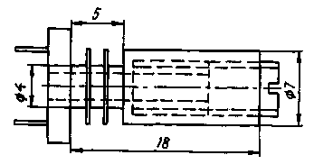
The windings of the AZ-T1 transformer contain nine turns of a bundle of three MGTF wires (nine turns are wound with six wires twisted together, and then the winding is divided into two parts - three wires each and connected in series). The windings of the transformer U1-T1 are wound simultaneously with three wires, and one of them (the one that will be included in the collector circuit of the transistor U1-VT6) is previously tapped from the middle. Coils Z2-L1 - Z2-L18 are wound on PTFE-4 frames (see Fig. 34). Size a between coils Z2-L2 and Z2-L3, Z2-L14 and Z2-L15, Z2-L17 and Z2-L18 - 5...6 mm, between Z2-L5 and Z2-L6, Z2-L8 and Z2- L9, Z2-L11 and Z2-L12 - 6...7 mm.
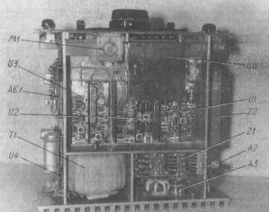
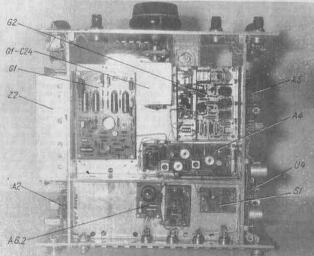
All chokes are unified, brand DM. The power transformer T1 is wound on a toroidal magnetic circuit with a cross section of 8,8 sq. cm made of transformer steel. Winding I contains 800 turns of wire PEV-2 0,65, winding II -72+72+72+72 turns PEV-2 1,2. The following types of electromagnetic relays are used for switching circuits: A1-K1 and Z1-K1 - Z1-K6 - RES48A (passport RS4.590.413); A1-K2 - RES52 (RS4.555.020); A2-K1 and G1-K2 - C1-K&<- RES55A (RS4.569.606); Z2-K1 - Z2-K12, G1-K1, A5-K2, A6-K1, A6-K2, U1-K1 and U2-K1 - RES49 (4.569.421-00-01); A5-K1 -RES60 (PC4.569.436). Range switch - small-sized PM-11P1N, type of work - PM-11P2N. The convenient chassis of the Ural-84 transceiver [7] was used as the basis for the design. The placement of the main components of the transceiver in it is explained in Figure 35 (top view) and Figure 36 (bottom view).
Between the sides of the chassis at a height of 65 mm from the bottom cover, a duralumin sub-chassis with dimensions of 225x150 mm is fixed, and at a height of 25 mm - another sub-chassis with dimensions of 225x80 mm, on which the A3 node board and the T1 power transformer are installed. Transistors A3-VT1, U3-VT2 and the U3-DA1 chip are installed on a common ribbed heat sink, which is also the rear wall of the chassis. setting; tanseiver start with power supply U4 (see fig. 16). First, with a trimmer resistor U4-R5, a voltage of 40 V is set at the output and they are convinced of its stability when the load current increases to 3A (the operating current of the protective device, if necessary, is changed by selecting the resistor U4-R7). Then they check the operation of the +15 V voltage regulator (it should remain practically unchanged when the load current increases to 1 A), after which the voltage is set to -4 V with a trimming resistor U12-R15 and its stability is checked when the load current increases to 0,1 A. Next, remove the frequency response of the AF amplifier with a CW filter (Fig. 10). In SSB mode, it should be uniform in the frequency band 300...3000 Hz. In CW mode, the bandwidth is narrowed to 6 Hz at an average frequency of 13 Hz with a tuning resistor A300-R800, and the total gain in both of these modes is equalized with a resistor A6-R22. IF amplifier 500 kHz (picture 8) tune together with the EMF by applying the AGC voltage of +5 V. By connecting the EMF input to the GSS and setting the RF voltage at the output of the latter with a frequency of 500 kHz and an amplitude of 5 μV, changing the capacitance of the tuning capacitors U3-C20, U3-C2 and the inductance of the coils U3-L2, U3-L1 ensure that the signal voltage at the output of the amplifier rises to about 5 mV. Further, by selecting the resistor U3-R4, the desired volume of self-listening in the TX mode is set, and the capacitor U3-C11 is the delay necessary to completely eliminate clicks in the phones when switching the transceiver from the TX mode to RX. The detector does not need to be adjusted. Establishment of the block of generators G2 (picture 7) start with a master oscillator on the elements of the IS G2-DD1. By selecting a resistor G2-R3, a capacitor G2-C1 and changing the capacitance G2-C2, they ensure that the generator starts up reliably and runs stably at the frequency of the G2-Z01 quartz resonator. Then, by adjusting the inductance of the coils G2-L1, a maximum voltage of 4,5 MHz is achieved on the capacitor G2-C8, and coils G2-L2 - a maximum voltage of 500 kHz on the capacitor G2-C10. Further, by selecting capacitors G2-C11 and U2-C10, U2-C11 (and, if necessary, the inductor U2-L4), they achieve a voltage of 2 MHz on the resistor U6-R4,5 within 3 ... 7 V. Selecting capacitors G2- C18, G2-C19, achieve the same voltage with a frequency of 500 kHz on the resistor, U3-R21, and by selecting the elements G2-L7, G2-C13 (in TX mode), and on the resistor A4-R11. Quartz filter unit U2 (picture 5) tune by adjusting the frequencies of the resonators U2-Z01, U2-Z02, U2-Z03 and U2-ZQ5 to the required values, lowering their resonant frequencies by a known method - by rubbing quartz plates with solder. This operation must be performed very carefully. The uniformity of the frequency response of the quartz filter in the frequency band of 5000 ... 5003 kHz is achieved by adjusting the inductance of the coils U2-L1 - U2-L3, and the suppression of "tails outside the passband of at least -40 dB" is achieved by connecting small capacitors parallel to the resonators U2-Z03, U2-Z04 capacitance (in Fig. 5 - capacitor C4 depicted by dashed lines). Setting PTD G1 (see figure 6) start with laying the boundaries of the ranges in accordance with the table. 1. Do this by selecting capacitors G1-C6, G1-C8, G1-C9, G1-C11, G1-C12, G1-C14, G1-C15, G1-C17, G1-C21, G1-C22 (taking into account the required TKE ) and changing the capacitance of the trimmer capacitors G1-C7, G1-C10, G1-C13, G1-C16, G1-C23. The 7 and 28 MHz bands are laid first. Further, by changing the voltage at the base and selecting the resistor G1-R14, the current through the transistor is set, at which the GPA signal is not distorted. In the GPU driver (picture 4) by selecting elements U1-C23, U1-C20, U1-R20, they achieve obtaining on the secondary winding of the transformer T1 stable in ranges and within each of them (when rebuilding the capacitor G1-C24) RF voltage with an amplitude of 3 ... 5 V, and by selecting the capacitor G1 -C18 in the GPA itself - the required range of its frequency detuning. Node PDF Z2 (picture 3) tune starting from the 1,9 MHz band. By connecting to the input of the node a 50-ohm output of the frequency response meter (for example, X1-48), and to the output - a 10 kΩ resistor with a 20 pF capacitor connected in parallel and a detector head of the frequency response meter, change; the capacitance of trimmer capacitors, and if necessary, by the selection of capacitors of constant capacitance connected in parallel to them, as well as a slight change; distances between the coils achieve a uniform frequency response in each range. After that, turn on the transceiver for reception (RX) and again, once again, specify the Setting of all circuits of the receiving path. At maximum gain, the sensitivity from the input of the transceiver with a signal-to-noise ratio of 10 dB should be about 0,05 μV. To eliminate possible errors, it is advisable to use a noise generator on a 2DZB lamp or the like during measurements. In the ranges of 21 and 28 MHz, maximum sensitivity is achieved by moving the trimmer resistor U1-R29. The maximum intermodulation dynamic range (100 dB) is achieved by adjusting the U1-L1C6C7 and U2-L1C2 circuits, as well as by careful selection of the U1-R5, U1-VD1, U1-R3, U1-C1 elements. AGC node A5 (picture 9) set up in this order. By applying a signal with a level from S3 to S9 points to the input of the transceiver, by changing the resistance of the tuned resistor A5-R3, the S-meter readings are "stacked" in the first half of the scale. Then the signal level is gradually increased from S9 to S9 + 80 dB and with the help of a tuned resistor A5-R2 do the same in the second half of the scale. In the process of these adjustments, the resistance of the resistor A5-R20 is selected in the emitter circuit of the transistor A5-VT7. If it is necessary to change the ratio of the S-meter readings in the first and second half of the scale, select the resistor A5-R14. Next, the speed characteristics of the AGC system are measured. Having soldered one of the terminals of the resistor A5-R12 from the board and connected an oscilloscope to the output of the node (pin 4), a signal with a level of S9 + 80 dB is fed to the transceiver input (jumpwise) The AGC voltage should decrease from the maximum value (+ 5 V) to the minimum ( +0,1...0,3 V) for no more than 0,2...0,5 ms. When the input signal is removed, it should return to the original level (+5 V) in about 25 seconds. With resistor A5-R12 in place, the reset time should decrease to 100ms. A further reduction in this time (to the optimum value) is achieved by selecting the capacitor A5-C8 when impulse noise is applied to the input of the transceiver. Table 2
In transmission mode (TX), tuning starts with a balanced modulator A4 (picture 11). First of all, the trimmer resistors A4-R9 (roughly), A4-R11 (fine) and the trimmer of the transformer A4-T1 achieve suppression of the reference signal by at least 50 ... 60 dB. Table 3
Further, when pronouncing a loud sound “a” in front of the microphone, the tuning resistor A4-R16 sets the DSB voltage of about 4 ... 1 V on the drain of the transistor A8-VT10. In the "Setting" mode, the CW generator on the A4-VT4 transistor is turned on, generating oscillations with a frequency of 501 kHz. By selecting the capacitor A4-C13 and adjusting the inductance of the coil A4-L1, a voltage of 4 ... 1 V is set on the drain of the transistor A6-VT8, subsequently focusing on the nominal output signal of the transceiver. The voltage on the circuit U2-L3C6 in this mode (with diodes U2-VD1, U2-VD2 off) should be about 6 ... .8 V, and at the input of driver A4 (pin 1) - 5 ... 6 mV. The required drain current of the transistor A2-VT5 (100 mA) is set by the trimmer resistor A150-R2. The output voltage of block A2 (at pin 30) must be within 2 ... 9 V. The required mode of operation of the transistor A3-VT1 (Fig. 13) - drain current 150 mA - set with a trimmer resistor A3-R4. The average signal voltage across the ranges at the dummy load with a resistance of 50 Ohms connected to the antenna jack of the transceiver should be about 36 V, which corresponds to an output power of 25 W. By ranges, the output power is equalized by the selection of resistor A3-R2 and capacitor A2-C2. If necessary, select the inductance (shifting or pushing the turns) of the coils Z1-L1 - Z1-L6. In conclusion, by selecting the resistor U4-R1, the device RA1 is calibrated (see figure 1) so that when working on the air, its arrow deviates to the last scale mark at a current of 2 A. In order to avoid overloading the amplifying stages, it is advisable to check the transceiver's transmission path using a two-tone signal. The author would like to thank Tulaev I.V. (UA4HK) and Baranov V.A. (RZ4HN ex UA4HNZ) for their great help in the development of the transceiver. Literature 1. Skrypnik V. A. Devices for monitoring and adjusting amateur radio equipment. - M.: Patriot, 1990. Author: Gennady Bragin (RZ4HK ex UA4HKB), Chapaevsk, Samara region; Publication: N. Bolshakov, rf.atnn.ru
Machine for thinning flowers in gardens
02.05.2024 Advanced Infrared Microscope
02.05.2024 Air trap for insects
01.05.2024
▪ Solar panels with human hair ▪ Global warming wakes up volcanoes ▪ NXP Unveils Ultra-Compact, High-Precision MEMS Frequency Synthesizer ▪ New Intel Pentium 4 processor
▪ section of the Antenna website. Article selection ▪ article Economics of the enterprise. Lecture notes ▪ article What is the smallest bird in Britain? Detailed answer ▪ article Universal probe. Encyclopedia of radio electronics and electrical engineering
Home page | Library | Articles | Website map | Site Reviews
www.diagram.com.ua |


 Leave your comment on this article: