|
|


 Arabic
 Bengali
 Chinese
 English
 French
 German
 Hebrew
 Hindi
Hindi Italian
 Japanese
 Korean
 Malay
Malay Polish
 Portuguese
 Spanish
 Turkish
 Ukrainian
 Vietnamese
|
ENCYCLOPEDIA OF RADIO ELECTRONICS AND ELECTRICAL ENGINEERING Pulse-width controllers of the KR1156EU2 and KR1156EUZ series. Reference data
Encyclopedia of radio electronics and electrical engineering / Reference materials Microcircuits of the KR1156EU2, KR1156EU3 series are designed to control switching secondary power supplies operating at a frequency of up to 1 MHz. The closest analogues of these microcircuits are UC3825 and UC3823 (Unitrode), respectively. The closest domestic analogue is KR1114EU4. Microcircuits are manufactured using planar epitaxial technology with p-n junction isolation. They are packaged in a sixteen-pin plastic case 2103.16-3 (Fig. 1). Weight of the device - no more than 1,2 g
The controllers are designed to work in devices with pulse-width (PW) control and voltage and current feedback. The signal propagation delay through the controller does not exceed 50 ns. The IC contains a broadband error amplifier with a slew rate of at least 12 V/µs and is compatible with input voltage feed-forward systems. At the output of the controllers, half-bridge switches for current up to 1,5 A (pins 11 and 14) are provided, which makes it possible to control powerful transistors of the MOS structure (in push-pull mode - KR1156EU2, in single-cycle mode - KR1156EUZ). Controllers contain a number of devices and systems that can significantly expand the scope. These include a SHI latch (more about it below), a current limiter in each period, a node that ensures smooth start of the controller, a limiter for the maximum duration of output pulses, a reference voltage source of 5,1 V. In addition, protection against reduced supply voltage, which has a "hysteresis", the ability to synchronize and turn off the controller with external signals. In the "Off" state, the microcircuit consumes a current of no more than 1 mA. Pinout of microcircuits (in parentheses the designation of the output on the conditional graphic image is indicated): pin. 1 - inverting input of the OU; pin. 2 - non-inverting input of the OS; pin. 3 (0ea) - output of the op amp, inverting the input of the SHI comparator; pin. 4 (Syn) - input/output of the synchronization signal; pin. 5 (Rt) - output for connecting a resistor* of the timing circuit; pin. 6 (Ct) - terminal for connecting a capacitor* of the timing circuit; pin. 7 (Ramp) - non-inverting input of the SHI comparator; pin. 8 (Cs) - output for connecting the capacitor of the soft start unit; pin. 9 (Stop) - input signal for current limiting or turning off the microcircuit; pin. 10 (Com) - common output, negative power output; pin. 11 (A) - output of the first half-bridge current amplifier; pin. 12 (Em) - emitter of current amplifier transistors; pin. 13 (Kol) - collector of current amplifier transistors; pin. 14 (B) - output of the second half-bridge current amplifier; pin. 15 (+U) - positive power output; pin. 16 (Uref) - output of the reference voltage source. The functional diagram of the KR1156EU2 microcontroller is shown in fig. 2. Since the KR1156EU2 and KR1156EUZ microcircuits have a lot of similarities, further in the text, unless otherwise stated, the description will refer to both.
The controller includes a sawtooth voltage generator G1, a 2 V bias voltage source G1,25, a controlled broadband error operational amplifier DA1, a SI comparator DA5, a latch on the DD3 trigger, a phase inverter on the DD5, DD6 triggers, output current amplifiers DA7, DA8 with logic control unit DD7, DD8, soft start unit (transistors VT1, VT2, current source G3), comparator load current limiter DA2 with a microcircuit shutdown unit (DA3, DD2), undervoltage blocking unit DA4, exemplary voltage source G4 with control unit this voltage (DA6). The protective functions of the controller are provided by a DA2 load current limiting comparator with a threshold voltage of 1 V, a DA3 chip turn-off comparator with a 1,4 V threshold voltage, and a soft start unit that can, in addition, limit the maximum duration of the output pulse (since the voltage at the output of the error amplifier DA1 limited by the voltage at the output of the controller 8 through the control circuit on the transistor VT1). The blocking unit of the controller, when the supply voltage drops below 9,2 V (with a "hysteresis" of 0,6 V) in the "Off" state, provides a low current consumption, while it switches the output amplifiers to a high-impedance state. Logic node DD7, DD8 prevents the simultaneous transition of the output amplifiers to a high level state and the appearance of many pulses during one cycle at the outputs A and B. Half-bridge output current amplifiers are designed to work with a load that has a large capacitive component, for example, gates of powerful MOS transistors, and are capable of delivering both incoming and outgoing current. Main technical characteristics*
* At a supply voltage of 15 V and an ambient temperature within 0O...+70 °C. **For the KR1156EUZ controller - by the period Maximum permissible values of characteristics*
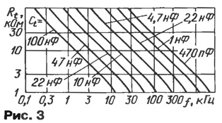
* The exposure time of the limit value of the parameter should not exceed 1 ms with a duty cycle of 100. ** At an ambient temperature greater than 25 °C, the dissipated power Р must be reduced according to the linear law Р = 1 - (Tacr.avg. - 25 °C) / Rt env.avr. where Rt env.avr - thermal resistance of the crystal-ambient , equal to 125 °C/W. The reference voltage source G4 consists of a thermally compensated stabilizer and a current amplifier that provides power to an external load with a current of up to 10 mA (from pin 16). The source is equipped with an output short circuit protection device at a level of about 30 mA. It powers the comparators, logic nodes, 1,25V bias, op amp, and sawtooth generator. The sawtooth voltage master oscillator can operate at frequencies up to 1 MHz. It is determined by the resistance of the resistor R, and the capacitance of the capacitor Ct of the timing circuit connected to terminals 5 and 6, respectively. At pin 5, the controller maintains a voltage of 3 V, and the current through the resistor Rt is reflected to pin 6 in a ratio of 1: 1, so the charging current l3Ct of the capacitor Ct is determined from the expression l3Ct = 3/Rt. At Rt = 3,65 kΩ and Ct = 1000 pF, the generator frequency is 400 kHz ±10%. To operate at a different frequency, it is necessary to change the parameters of the timing circuit in accordance with Fig. 3.
The "dead" time of the oscillator, which is equal to the duration of the pulse at the output Syn and determines the dynamic range of the controller (since the outputs A and B are at the same time in a low state), depends on the capacitance Ct and can reach 100 ns. The generator generates a sawtooth voltage at the Ct input (pin 6), a synchronization signal for the joint operation of two controllers (taken from pin 4), generates clock pulses at pin 4 during the sawtooth voltage drops to simultaneously close the output amplifiers in order to exclude through current (through transistors amplifiers) and switches the latch DD3 to a state that allows the operation of the output amplifiers. The generator is built according to the Schmitt trigger circuit, the output of which is connected to pin 4 through an emitter follower on an npn transistor. Clock pulses are formed on this pin, their low level (2,3 V) corresponds to the charging of the capacitor Ct, and high (4,5 V) - detente. The emitter follower allows you to combine the outputs of 4 several microcircuits (wiring OR). The load capacity of the output is 4 - 1 mA, and since the internal current source in the load of the emitter follower consumes no more than 400 μA, the branching factor for this output during synchronous operation with similar microcircuits is at least two. The generator of the slave (synchronized) microcircuits can not be blocked, but tuned to a frequency slightly lower than that of the master generator, by appropriately choosing the timing elements Rt and Ct. With this approach, each controller will have a local sawtooth voltage. It is also possible to completely turn off the generator if pin 5 is connected to pin 16, and pin 6 to a common pin. In this case, the synchronization signal is supplied from an external generator to pin 4. For more branched synchronization, an emitter follower controlled by the clock signal of the master controller can be used, and slaves can be connected to its output through capacitors and, if necessary, through terminating resistors and transmission lines. The correct choice of capacitor Ct is very important. At high frequency, its effective series resistance and inductance, as well as the dielectric absorption value, determine the frequency accuracy and stability of the oscillator. Therefore, it is recommended to use only RF capacitors. To reduce the influence of the parasitic inductance of the capacitor leads, it is necessary to shorten them as much as possible during installation and connect them as close as possible to pin 10 of the microcircuit. Single-level sync pulses translate the DD3 latch to the zero state, clock the phase inverter and strobe the output amplifiers of the controller, preventing through current. At the zero level of the sync pulse, a high-level pulse appears at the output of one of the amplifiers and remains until the next sync pulse arrives, if there was no inhibition in other circuits. The error signal amplifier DA1 is a broadband high-speed op-amp with a low-resistance output. The use of only n-p-n transistors in its signal path made it possible to achieve a unity gain frequency of 5,5 MHz. To ensure the minimum time for the error signal to pass through the op-amp, the collector junction of the corresponding transistors is shunted with a Schottky diode to prevent saturation. The gain is set, as usual, by choosing the OS depth. The typical frequency response of the amplifier has a gain value of 95 dB at zero frequency and one pole at 100 Hz. Connecting the inputs of the error amplifier DA1 depends on the polarity of the output voltage of the designed power supply. If it is required to obtain a stabilized positive voltage (relative to the common wire), then the common mode voltage is 5,1 V (exemplary) and the OS circuit is built as shown in Fig. 4a. When negative, the common-mode voltage is recommended to be set equal to half the exemplary one, and the OS circuit divider is connected between the output of the power source and terminal 16 of the controller (Fig. 4, b).
The emitter of the transistor VT1 is connected to the base of the output npn transistor of the op-amp (according to the diagram in Fig. 2) of the p-n-p structure. Therefore, the voltage at the output of the op amp cannot exceed the voltage at pin 8 of the controller. It should be borne in mind that the output of the op amp is loaded with an internal 50 ohm resistor connected to the common output. Therefore, if the external load involves a large sink current, an additional shunt resistor may be required to reduce the voltage at the output of the op-amp. SHI comparator DA5 is made according to the scheme of a differential amplifier based on npn transistors with an emitter follower at the output, which prevents the saturation mode of the comparator transistors. The output signal corresponds to the ESL at a supply voltage of 5,1 V. The common-mode input signal of the comparator is lower-limited by a value of approximately 1 V. Since the voltage at the Ramp input of the controller (for example, when a sawtooth voltage is applied to it from pin 6) can vary from 0 to 3 V, for level matching, a voltage shift of 1,25 V is provided at the non-inverting input of the comparator by the internal bias source G2. The current limiting comparator DA2 is similar in structure to the SHI comparator. The DA3 turn-off comparator is made according to the scheme of a differential amplifier based on p-n-p transistors. A fixed voltage of 1 and 1,4 V, respectively, formed from the reference voltage, is applied to the inverting input of these comparators. The logic elements on the signal path through the controller, including the SHI latch DD3 and the phase inverter DD5, DD6, are made on the ESL with buffer emitter followers. The switching current of these nodes is chosen quite large - 400 μA. Therefore, although there are two OR elements (DD1 and DD4), OR-NOT elements (DD7, DD8), latch (DD3) on the way between the input comparators and output current amplifiers, their share in the total delay time does not exceed 20% The main delay is comparators and output amplifiers. However, how fast the signal would not pass through the path means little if the output does not provide fast switching with the required amplitude. The output half-bridge current amplifiers DA7, DA8 allow you to switch a load with a capacity of 1000 pF for 30 ns at a controller supply voltage of 15 V. The peak value of the current through the load is at least 1,5 A. To ensure the speed of the amplifiers, one has to put up with a through current through the output transistors, due to which, in particular, the microcircuit heats up, especially at high frequencies. In the output stage of the KR1156EU2 controller, powerful output transistors are controlled by a complementary signal, i.e. when one is open, the other is closed. The mode of operation of the transistors is chosen so that only 20 ns of through current flows through them during each switching, which at a frequency of 500 kHz adds only 10 mA to the consumed current. This figure is the result of a compromise; it is easy to achieve zero through current, but in this case the total delay becomes unacceptably large. If the controller supply voltage becomes less than a certain value (equal to the operation voltage minus the "hysteresis" voltage), the undervoltage protection comparator DA4 is activated. The low level from its output by the element AND-NOT DD9 is inverted into a high one and fed to the input of the elements OR-NOT DD7, DD8, which invert it again. As a result, the output amplifiers DA7, DA8 go into a low level state. A high level from the DD9 element also comes to the input of the OR element DD2, opening the transistor VT2, which discharges the soft start capacitor in the output circuit 8. The transistor VT1, which opens at the same time, reduces the voltage at the output of the op-amp DA1 to almost zero. At the same time, a low level from the output of the comparator DA4 turns off the reference voltage source, after which the output amplifiers go into a state with a high output impedance. If now the supply voltage, increasing, becomes greater than the operation voltage of the DA4 comparator, it switches, a high level from its output goes to the DD9 element, to the exemplary source G4 and gradually puts the controller into operating mode. As soon as the voltage at the output of the exemplary source, increasing, exceeds 4 V, the reference voltage control comparator DA6 is activated. Now both inputs of the DD9 element are high, and the output is low. This removes the prohibition on the passage of the signal through the elements DD7, DD8, generates a low level at the output of the DD2 element, which (if the output of the comparator DA3 is also low) closes the transistor VT2 and smoothly starts the controller. When the power supply is turned on, the current through the powerful switching transistors is determined by the load current and the charging current of its output capacitance, and at the first moment it is much higher than the nominal value. To prevent the associated overload of the output amplifiers, a node consisting of a transistor VT1 and a soft start capacitor was introduced into the controller. The node slowly increases the output voltage of the op amp DA1 from almost zero to the nominal value, and hence the duration of the pulses at outputs A and B. When the controller is in micropower mode or the voltage at pin 9 is greater than 1,4 V, the capacitor in the pin 8 circuit is discharged and there are no output pulses. The soft start capacitor is charged by current source G3 (9 µA). The increasing output voltage OV DA1 SHI comparator is compared with the sawtooth voltage at the direct input and generates pulses increasing in duration at the output. At first, the opening time of the output amplifiers is small and the current through them is less than the critical one. As soon as the output voltage reaches the nominal level, the stabilization circuit will turn on. Transistor VT1 will close. In addition to the main purpose, the soft start unit can be used for other purposes. So, the ability of the controller to limit the voltage at the output of the op amp allows you to limit the maximum opening time of the output transistors in traditional power supplies, and in the current mode - to program the level of the maximum peak current. Typical inclusion of the controller using the example of a five-volt stabilized power supply operating within the input voltage of 42 ... 56 V with a load current of 1 ... 10 A is shown in fig. 5 [1].
With an increase in load current, as soon as the voltage on the current sensor R12, supplied to the Stop input of the controller, exceeds 1 V, its current limiting comparator DA2 will work and a single drop, passing through the element DD1, will set the SHI latch DD3 to state 1. This voltage will close the output amplifiers, at least until the end of the current period. The latch has priority on the input S, so its transition to the zero state is possible only after the removal of the current overload. If the output of the power supply is closed, then due to the fact that the output transistors are turned off in a time of about 100 ns, the current through the transistors VT1, VT2 of the source has time to increase to the second value, at which the turn-off comparator DA3 of the microcircuit will work. As a result, the soft start capacitor C4 will be discharged and the transistor VT1 of the controller will reduce the voltage at the output of the op-amp to almost zero. After closing the powerful transistors VT1, VT2, the voltage at terminal 9 of the controller will become close to zero and the soft start process will begin. If the output closure is not removed, the described process will be repeated. The logical node for controlling the output amplifiers of the controller provides the following functions: their simultaneous closing at a high level of the synchronizing pulse at pin 4 or at the output of the latch; their alternate opening at a low level of the sync pulse and at the output of the latch; change in the duration of the output pulses depending on the level of the error signal. In the power supply (Fig. 5), the usual SHI regulation is used, when the OS voltage is connected to the inverting input of the controller DA1 op-amp, and the exemplary one to the non-inverting one. The error signal creates a certain voltage at the output of the op-amp, which comes to the inverting input of the comparator DA5. The non-inverting input of the comparator (pin 7) through the R2C3C6 circuit receives a sawtooth voltage from the generator G1 (pin 6), shifted upward by the source G2. The push-pull cycle starts when the controller output clock G1 is high. This pulse sets a low level at the latch output and at the same time, passing through the DD4 element to the input C of the phase inverter DD5, DD6, switches it to the next state and prepares the corresponding output amplifier for opening. In addition, it comes directly to the inputs of the elements DD7, DD8. Consequently, the outputs of both amplifiers DA7, DA8 are low, and the source transistors VT1 and VT2 are closed. After the decay of the clock pulse, a low level from the output of the DD4 element removes the prohibition on opening the output amplifiers. That powerful source transistor for which there is an enabling signal from the phase inverter opens. At the same time, charging of the capacitor C1 begins and the voltage at terminal 7 of the controller increases. As soon as the sawtooth voltage at the non-inverting input of the comparator equals the level of the error signal at the inverting input, the output will go high, which will set the latch to a one state. An open powerful source transistor closes, and a closed one is blocked from accidental opening. These transistors will be closed until the end of the period, until the master oscillator sets the latch output to a low level with the next sync pulse and, by switching the phase inverter to the next state, prepares another powerful transistor to turn on. Further, the described processes are repeated. Depending on the level of the error signal, the comparator switches later or earlier. The on-time of the output amplifier also changes accordingly. This is how the output voltage of the converter is stabilized. The controller can generate a push-pull pulse-width signal to control high-power transistors in two main modes. In the first one, the comparator compares the output voltage of the error amplifier with the sawtooth voltage at pin 6. This is the traditional voltage feedback mode. In the second, the comparator compares the voltage of the error amplifier with the voltage drop across the resistor R12 - a current sensor included in the common circuit of powerful switching transistors (current feedback mode). In the case under consideration, as can be seen from Fig. 5, a combination of these two modes is applied. To suppress switching noise, an integrating circuit R4C5 is used between the current sensor and the Stop input. In the case when energy losses do not allow the use of a current-measuring resistor, a current transformer is used. If the converter must operate with input voltage that varies over a wide range, it is advisable to use a direct parametric connection for the input voltage. The parametric sawtooth voltage applied to the input of the comparator is generated by an external RC circuit. The falling section of the "saw" is formed by a signal at the output of the generator by an external transistor. To prevent saturation of the converter transformer, a node can be used that calculates the volt-second product and turns off the power transistors when it reaches a dangerous level. It is recommended to shunt outputs A and B of the controller with Schottky diodes (VD2, VD3) for a pulsed current of at least 2 A. If the controller is loaded with an isolation transformer or the current surges through the drain-gate capacitance are very high, shunt diodes are required. They will limit negative spurious pulses on outputs A and B to 0,3 V. Like all high-frequency components, the controller requires careful attention to the placement of external (attachment) components and wiring in order to minimize parasitic inductive or capacitive coupling. The leads of the parts must be shortened as much as possible. For these reasons, it is preferable to mount the controller on a double-sided printed circuit board. Signal conductors are placed so that they are everywhere located above the foil of the common wire. The power outputs should be shunted with two pass-through capacitors - a ceramic low-inductance capacitance of 0,1 μF, placed no further than 6 mm from pin 15 of the microcircuit, to suppress high-frequency interference and an oxide (tantalum) rating from 1 to 5 μF, soldered no further than 12 mm from pin 13 and playing the role of an energy storage device for powering output amplifiers. It is recommended to connect a low-inductance capacitor with a capacity of at least 0,01 uF between terminal 16 and the common wire. To increase the stability of the converter against parasitic excitation, the series parasitic inductance of the output of the current amplifiers of the controller should be minimal. The solution here can be the approximation of powerful field-effect transistors to the microcircuit as far as possible and the use of series damper non-inductive resistors R7, R8. To reduce the influence of powerful transistors on analog circuits, shielding and the use of consistent lines for transmitting control pulses to their gate are required. Neither in foreign nor in domestic documentation, the type of powerful field-effect transistors VT1, VT2 and Schottky rectifier diodes VD6 of the converter is indicated. Those who want to make it themselves will have to experimentally select these components and make sure that the device works reliably. We can recommend transistors KP750A, KP767V, KP778A, IRF640. In addition to the type of powerful diodes indicated in the diagram, KD271BS, KD272BS, KD273BS, KDSh2967BS, KDSh2967VS, CTQ2535, CTQ2545 can be suitable; diodes VD4, VD5 - from the 2D253 series, as well as 2D255V-5, ZDCH122-20, ZDCH122-20X. Before work, you should definitely familiarize yourself with [2]. The KR1156EUZ controller differs from the one described by the absence of a phase inverter trigger and by the fact that the output current amplifiers operate in antiphase. In addition, versions are available with common-mode outputs A and B, which can be connected in parallel, with one output B (as in the UC1823) and with output A connected to the inverting input of the current limiting comparator. Literature
Author: S.Egorov, Bryansk
A New Way to Control and Manipulate Optical Signals
05.05.2024 Primium Seneca keyboard
05.05.2024 The world's tallest astronomical observatory opened
04.05.2024
▪ Biodegradable wireless subcutaneous charger ▪ Smartphone Samsung Galaxy W with 7" screen 1280x720 ▪ Brain implants to restore vision ▪ Three human brains tied into a net ▪ By evening the brain shrinks
▪ section of the site Standard instructions for labor protection (TOI). Selection of articles ▪ article Out of this world. Popular expression ▪ article Which stars are closest to Earth? Detailed answer ▪ Pepino article. Legends, cultivation, methods of application ▪ article Simple transistor tester. Encyclopedia of radio electronics and electrical engineering ▪ article The Incredible Knot. Focus Secret
Home page | Library | Articles | Website map | Site Reviews
www.diagram.com.ua |


 Leave your comment on this article: