Diode assembly KD638AS. Encyclopedia of radio electronics and electrical engineering

Encyclopedia of radio electronics and electrical engineering / Reference materials
 Comments on the article
The assembly of high-power silicon diodes KD638AS is made using epitaxial-planar technology. The assembly is composed of two diodes having a common cathode terminal. The device is intended for use in switching power supplies and other equipment units of wide application.
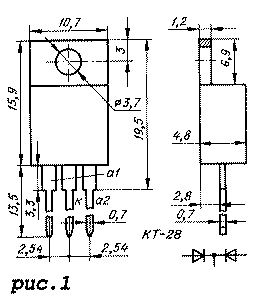
The diode assembly is framed in a plastic case KT-28 with rigid plate leads (Fig. 1), the mass of the device is no more than 2.5 g. The foreign analogue is BYV16-200T.
Main technical data at Tav.av.= 25°C (for one diode)
| Constant reverse diode current at reverse voltage 200V, no more |
5 μA |
| Constant forward voltage of the diode at direct current 8A, no more |
In 1.25 |
| Diode reverse recovery time at forward current 1A, reverse voltage 30V, forward current decrease rate 50A/µs and reverse current equal to 0.25 of its maximum value, no more |
35 ns |
| Thermal resistance, transition-housing for the assembly as a whole, no more |
1.3 °C/W |
Limit values
| The highest constant reverse voltage of the diode |
In 200 |
| The largest average forward current of the diode with simultaneous operation of the second diode in the same mode |
A 8 |
| Highest junction temperature |
150 °C |
| Limits of the operating range of the ambient temperature |
-60 ... + 100 °C |
| Permissible value of static potential* |
In 500 |
|
| *IV degree of rigidity according to OST 11073.062 |
It is not allowed to operate diodes at the limit values of two or more parameters. When mounting the assembly on the board, no more than two times bending of the leads is allowed at a distance of at least 5 mm from the edge of the case at an angle of 90 degrees. with a radius of curvature of at least 1.5 mm (it is not allowed to bend the terminals in the plane of the body). In this case, it is necessary to take measures that exclude the transfer of force to the body.
The distance from the housing to the place of tinning and soldering of the leads must not be less than 5 mm. The allowable number of resoldering of the assembly leads during installation and adjustment operations is three.
In order to reduce the thermal resistance of the housing-heat sink, it is recommended to use a heat-conducting paste, for example, KPT-8 (GOST 19783). Do not solder the assembly's heat sink plate to the heat sink. If it is necessary to isolate the assembly from the heatsink, the increase in junction-heatsink thermal resistance caused by the insulating pad (or paste) must be taken into account.
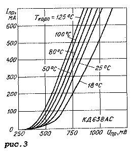
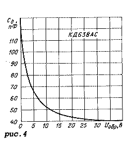
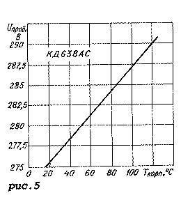
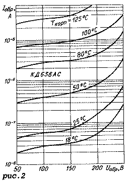
Graphic dependences of the parameters of the KD638AS diode assembly are shown in Fig. 2-5. Figure 2 shows the dependences of the DC reverse current on the DC reverse voltage, and Figure 3 shows the current-voltage characteristics at various case temperatures. The dependence of the diode capacitance on the constant reverse voltage is shown in Fig. 4, and the temperature dependence of the breakdown voltage is shown in Fig. 5.
Publication: N. Bolshakov, rf.atnn.ru
 See other articles Section Reference materials.
Read and write useful comments on this article.
<< Back
 Latest news of science and technology, new electronics:
Traffic noise delays the growth of chicks
06.05.2024
The sounds that surround us in modern cities are becoming increasingly piercing. However, few people think about how this noise affects the animal world, especially such delicate creatures as chicks that have not yet hatched from their eggs. Recent research is shedding light on this issue, indicating serious consequences for their development and survival. Scientists have found that exposure of zebra diamondback chicks to traffic noise can cause serious disruption to their development. Experiments have shown that noise pollution can significantly delay their hatching, and those chicks that do emerge face a number of health-promoting problems. The researchers also found that the negative effects of noise pollution extend into the adult birds. Reduced chances of reproduction and decreased fertility indicate the long-term effects that traffic noise has on wildlife. The study results highlight the need ... >>
Wireless speaker Samsung Music Frame HW-LS60D
06.05.2024
In the world of modern audio technology, manufacturers strive not only for impeccable sound quality, but also for combining functionality with aesthetics. One of the latest innovative steps in this direction is the new Samsung Music Frame HW-LS60D wireless speaker system, presented at the 2024 World of Samsung event. The Samsung HW-LS60D is more than just a speaker system, it's the art of frame-style sound. The combination of a 6-speaker system with Dolby Atmos support and a stylish photo frame design makes this product the perfect addition to any interior. The new Samsung Music Frame features advanced technologies including Adaptive Audio that delivers clear dialogue at any volume level, and automatic room optimization for rich audio reproduction. With support for Spotify, Tidal Hi-Fi and Bluetooth 5.2 connections, as well as smart assistant integration, this speaker is ready to satisfy your ... >>
A New Way to Control and Manipulate Optical Signals
05.05.2024
The modern world of science and technology is developing rapidly, and every day new methods and technologies appear that open up new prospects for us in various fields. One such innovation is the development by German scientists of a new way to control optical signals, which could lead to significant progress in the field of photonics. Recent research has allowed German scientists to create a tunable waveplate inside a fused silica waveguide. This method, based on the use of a liquid crystal layer, allows one to effectively change the polarization of light passing through a waveguide. This technological breakthrough opens up new prospects for the development of compact and efficient photonic devices capable of processing large volumes of data. The electro-optical control of polarization provided by the new method could provide the basis for a new class of integrated photonic devices. This opens up great opportunities for ... >>
| Random news from the Archive Laser using the effect of superconductivity
08.02.2018
In Silicon Valley, a place known as the home of all the latest high technology and innovation, construction has begun on a new X-ray laser that is 3 miles (4,8 kilometers) long and uses a mass of superconducting components. This laser is being built at the Fermi National Laboratory's SLAC National Linear Accelerator Laboratory, where the first cryogenic section has just been delivered.
The 12.2 meter (40 ft) sections, called cryomodules, are the "building blocks" of the future LCLS-II laser, which will replace the existing Linac Coherent Light Source X-ray free electron laser (LCLS). The modules have a series of cryogenic units made of niobium. These knots will form electric fields of special shape and great strength, which will accelerate the electrons to almost the speed of light. The LCLS-II laser will produce pulses 10 times brighter than those produced by the LCLS laser. In this case, the pulse repetition rate will be a million times per second.
Half of the new laser's cryomodules will be made at Fermi National Laboratory and the other half at the Thomas Jefferson National Accelerator Center in Virginia. Initially, each of the created modules will be tested individually at the place of its assembly, after which it will be sent to Silicon Valley. These modules will be installed in the tunnel formerly occupied by the SLAC laser equipment, which is 2 miles long and 10 meters below the ground.
Thanks to the amazing performance of the new laser, scientists will be able to study complex materials and processes with unprecedented resolution. The light from the new laser will make it possible to see rare and transient chemical phenomena, study the work of molecules of biological origin, look into the strange world of quantum mechanics and measure the motion parameters of individual components of molecules and even atoms.
|
Other interesting news:
▪ Video card GeForce GTX 960
▪ Energy storage in microchips
▪ Anti-clot magnet
▪ NetApp AFF8000 Flash Arrays
▪ Potato bacterium antibiotic
News feed of science and technology, new electronics
 Interesting materials of the Free Technical Library:
▪ section of the site Experiments in chemistry. Article selection
▪ article Well-intentioned speeches. Popular expression
▪ article In which state is mail addressed not by streets and house numbers, but by their descriptions? Detailed answer
▪ article Gageya yellow. Legends, cultivation, methods of application
▪ article Imitator of sounds of a drop. Encyclopedia of radio electronics and electrical engineering
▪ article Generator of test signals for testing UMZCH. Encyclopedia of radio electronics and electrical engineering
Leave your comment on this article:
 All languages of this page
Home page | Library | Articles | Website map | Site Reviews

www.diagram.com.ua
2000-2024


 Arabic
 Bengali
 Chinese
 English
 French
 German
 Hebrew
 Hindi
Hindi Italian
 Japanese
 Korean
 Malay
Malay Polish
 Portuguese
 Spanish
 Turkish
 Ukrainian
 Vietnamese