 Free technical library
Sticky stick. Focus Secret

Directory / Spectacular tricks and their clues
 Comments on the article
Focus Description:
To prove that you have magical powers, place your wand or pencil in the palm of one hand, facing away from the audience. Slowly remove your fingers: the stick seems to stick to your hand, as if it were being held by a magnetic field.
Focus secret:
The combination of moving the wand or pencil in different directions will give the impression that they "stick" to the magician's fingers with the help of magic.
Hold the wand between your palms (fig. 1).
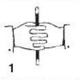
Raise one thumb (fig. 2).

The audience still thinks your second thumb is holding the stick. Then lift the second thumb (fig. 3). They will be amazed!

Looking at figures 4 and 5, you will see how the trick is performed.


Gently fold your fingers so that one of them is inside the palms (see Fig. 4). The wand is held by this hidden finger. When you are done demonstrating the trick, quickly extend your arms forward and let the stick fall.
 We recommend interesting articles Section Spectacular tricks and their clues:
▪ Spoon on the nose
▪ Mysterious squares
▪ Playing card manipulation
 See other articles Section Spectacular tricks and their clues.
Read and write useful comments on this article.
<< Back
 Latest news of science and technology, new electronics:
Machine for thinning flowers in gardens
02.05.2024
In modern agriculture, technological progress is developing aimed at increasing the efficiency of plant care processes. The innovative Florix flower thinning machine was presented in Italy, designed to optimize the harvesting stage. This tool is equipped with mobile arms, allowing it to be easily adapted to the needs of the garden. The operator can adjust the speed of the thin wires by controlling them from the tractor cab using a joystick. This approach significantly increases the efficiency of the flower thinning process, providing the possibility of individual adjustment to the specific conditions of the garden, as well as the variety and type of fruit grown in it. After testing the Florix machine for two years on various types of fruit, the results were very encouraging. Farmers such as Filiberto Montanari, who has used a Florix machine for several years, have reported a significant reduction in the time and labor required to thin flowers.
... >>
Advanced Infrared Microscope
02.05.2024
Microscopes play an important role in scientific research, allowing scientists to delve into structures and processes invisible to the eye. However, various microscopy methods have their limitations, and among them was the limitation of resolution when using the infrared range. But the latest achievements of Japanese researchers from the University of Tokyo open up new prospects for studying the microworld. Scientists from the University of Tokyo have unveiled a new microscope that will revolutionize the capabilities of infrared microscopy. This advanced instrument allows you to see the internal structures of living bacteria with amazing clarity on the nanometer scale. Typically, mid-infrared microscopes are limited by low resolution, but the latest development from Japanese researchers overcomes these limitations. According to scientists, the developed microscope allows creating images with a resolution of up to 120 nanometers, which is 30 times higher than the resolution of traditional microscopes. ... >>
Air trap for insects
01.05.2024
Agriculture is one of the key sectors of the economy, and pest control is an integral part of this process. A team of scientists from the Indian Council of Agricultural Research-Central Potato Research Institute (ICAR-CPRI), Shimla, has come up with an innovative solution to this problem - a wind-powered insect air trap. This device addresses the shortcomings of traditional pest control methods by providing real-time insect population data. The trap is powered entirely by wind energy, making it an environmentally friendly solution that requires no power. Its unique design allows monitoring of both harmful and beneficial insects, providing a complete overview of the population in any agricultural area. “By assessing target pests at the right time, we can take necessary measures to control both pests and diseases,” says Kapil ... >>
| Random news from the Archive Silicon retains conductivity at ultra-low charge levels
01.03.2020
Researchers from the American National Institute of Standards and Technology (NIST) have come up with a new method for measuring the mobility of charged particles in silicon, which, if not overturned, then significantly expanded the understanding of charge transfer processes in semiconductors.
The method proposed by the scientists made it possible to carry out the most sensitive measurements of the speed of movement of an electric charge in silicon, and this is an indicator of its effectiveness as a semiconductor. As a result, the new method will make it possible to more accurately assess the effect of certain dopants on the silicon conductivity and will form the basis for improving the characteristics of semiconductor devices. This is a chance to improve the performance of the chips almost for nothing only through a better understanding of the processes. Carry out tuning, so to speak.
Traditionally, the mobility of electrons and holes in silicon was measured by the Hall method. This method assumes that contacts are soldered on a sample of silicon (semiconductor) to pass an electric current. The disadvantage of this method is that defects or impurities appear at the soldering points, which introduce distortions into the measurement results.
For the purity of the experiment, scientists from NIST used a non-contact method. The silicon sample was first exposed to light of low intensity in the form of ultrashort pulses of visible light, and then the sample was irradiated with radiation pulses in the far infrared or microwave range. Weak visible light produced a photodoping effect on silicon: charged particles appeared in the silicon layer in the form of electrons and holes.
Visible light, for obvious reasons, could not penetrate into the thickness of silicon. For this purpose, the photodoped sample was irradiated with terahertz radiation (in the far infrared range), for which silicon is transparent. And the more charged particles in the sample, the more light penetrates or is absorbed by the sample. It is important to note here that for a more accurate measurement of the electron mobility in the sample, its thickness should have been quite large, up to 1 mm. This ruled out the influence of defects on the sample surface on measurements.
However, the number of electrons and holes "introduced" by visible light in the sample had to be as small as possible in order to lower the sensitivity threshold during measurements. Usually, for this, the sample was irradiated with one photon, but in the case of a thick sample, one photon knocked out insufficiently charged particles in silicon. A way out was found in irradiating the sample with two photons of visible light. After that, terahertz radiation freely passed through the sample with a minimum number of charged particles in the bulk of the material. According to scientists, the threshold of sensitivity was reduced by a factor of 10 from 100 trillion charge carriers per cm2 to 10 trillion.
As soon as the threshold of sensitivity was lowered, the surprising became clear. The mobility of electrons in silicon turned out to be able to grow even to a very rarefied state of carriers in the material, which no one suspected before. Actually, the mobility itself turned out to be 50% higher than previously thought. For a control check, a similar experiment was carried out with gallium arsenide (GaAs), also a photosensitive semiconductor. It was found that the mobility of charge carriers in this material continues to grow as their density decreases. The carrier density limit measured by the new method turned out to be about 100 times lower than previously thought.
In the far or not so far future, semiconductors will be able to operate at very low charge levels. At least the theoretical limit has been pushed far enough. These are highly sensitive solar panels, and single-photon detectors (hello to quantum computers!), ultra-efficient electronics and much more.
|
Other interesting news:
▪ The magnet turns the material from soft to hard
▪ All the most valuable companies in the world are from the IT sector
▪ Age of Democracy
▪ Keyboard for extreme conditions on the FDC2214 capacitance meter
▪ Immunity saves tattoos
News feed of science and technology, new electronics
Interesting materials of the Free Technical Library:
▪ site section Chargers, accumulators, batteries. Article selection
▪ The road to hell is paved with good intentions. Popular expression
▪ article What is silicon? Detailed answer
▪ article Working on a risograph. Standard instruction on labor protection
▪ Article LDS is battery powered. Encyclopedia of radio electronics and electrical engineering
▪ article Amazing smoke. Focus Secret
Leave your comment on this article:
 All languages of this page
Home page | Library | Articles | Website map | Site Reviews

www.diagram.com.ua
2000-2024


 Arabic
 Bengali
 Chinese
 English
 French
 German
 Hebrew
 Hindi
Hindi Italian
 Japanese
 Korean
 Malay
Malay Polish
 Portuguese
 Spanish
 Turkish
 Ukrainian
 Vietnamese