|
|


 Arabic
 Bengali
 Chinese
 English
 French
 German
 Hebrew
 Hindi
Hindi Italian
 Japanese
 Korean
 Malay
Malay Polish
 Portuguese
 Spanish
 Turkish
 Ukrainian
 Vietnamese
|
ENCYCLOPEDIA OF RADIO ELECTRONICS AND ELECTRICAL ENGINEERING TVs on LCD panels. LCD panels (LCD). Encyclopedia of radio electronics and electrical engineering
Encyclopedia of radio electronics and electrical engineering / Телевидение The dream of "flat" TVs and monitors, having a very small size in depth, arose more than one decade ago. But only in recent years it has become a reality: serial models appeared on flat display panels. Cathode-ray tubes (kinescopes), which serve as the basis of any TV, have existed for many decades and are constantly being improved. However, they also have disadvantages: the presence of high voltage, large volumetric dimensions (especially depth at large image sizes), etc. Therefore, developers have always strived for new ideas when creating display devices. One of them is the use of a liquid crystal substance as a valve for transmitting light fluxes. Finally, this idea was embodied in the form of LCD displays (panels) - LCD (Liquid Crystal Display). The rapid growth of their production abroad has led to the emergence of both a large number of models of "flat" TVs and computer monitors. Consider the principle of operation and design options for such displays [1,2]. In general, it is known that an LC substance (material) modulates an external light flux under the action of an electric field or current. The specific operation of LCD displays is based on the use of the effect of rotation of the plane of polarization of the light flux by a layer of nematic LC substance (the so-called twist effect). The design of the LCD panel is shown in fig. one.
The panel contains two plane-parallel substrates made of a transparent material (usually glass with a thickness of about 1 mm), located one relative to the other with a fixed gap, into which the LC material is inserted. On the inner sides of the substrates, addressing electrodes are applied in the form of a certain pattern. Indium oxide film is used as a transparent conductive layer of electrodes. Layers of orienting coatings deposited on addressing electrodes are designed to set a certain orientation of LC molecules in the working material. The gap between the substrates is set by calibrated spherical or cylindrical spacer elements (spacers), the diameter of which can be within 3...25 µm. After assembly (gluing), the panel is sealed around the entire perimeter, and the sealant layer also has spacers. Polaroids with a certain orientation of the polarization plane are pasted onto the outer sides of the substrates. The principle of operation of the LCD cell (pixel) of the panel using the twist effect is illustrated in Fig. 2.
Molecules of the LC material have a dipole moment. As a result of the interaction of the electric fields of the dipoles, a spiral structure is formed from the molecules of the LC substance. The layers of orienting coatings on the upper and lower substrates, together with the dipole structure of the LC material, in the absence of an electric field, provide a rotation of the plane of polarization of the light flux by 90°. A layer of a nematic LC substance oriented in this way has the property of polarization of the light flux passing through it. The planes of polarization of the upper and lower polarizing filters are rotated relative to each other by 90°. As seen in fig. 2a, the light flux first passes through the upper polarizing filter. In this case, its half, which does not have azimuthal polarization, is lost. The rest of the already polarized light, passing through the layers of the LC material, rotates the plane of polarization by 90°. As a result, the orientation of the plane of polarization of the light flux will coincide with the plane of polarization of the lower filter, and the flux will pass through it practically without loss. If an LC substance is placed in an electric field, applying a voltage to the addressing electrodes as shown in Fig. 2,6, the helical molecular structure in it collapses. The light flux passing through the LC material no longer changes the plane of polarization and is almost completely absorbed by the lower polarizing filter. Consequently, an LC substance has two optical states: transparent and opaque. The ratio of the transmittances in both states determines the contrast of the image. To control the optical state of the pixel cells (image elements) of the panel, it is necessary to generate such voltages on the addressing electrodes so that the state of each pixel changes without changing the state of others. Based on this, the topology of the addressing electrodes of the LCD panel is a matrix formed by a system of row and column electrodes, structurally located on two parallel transparent substrates. Elements (pixels) of the television image in the LCD panel are formed at the intersection of line and column electrodes. To implement the control of a large number of picture elements (and in TVs this is almost always the case), signal multiplexing is used. Several options for the topology of matrices used in LCD panels are shown in Fig. 3.
The variant in fig. 3a is the simplest and most popular. The variant in fig. 3,6 allows you to get a wider pin pitch for supplying columnar control signals. The options in fig. 3, in ig - a variation of the Dual Scan (or Dauble Scan) architecture, which provides a reduction in the number of multiplexed lines, which makes it possible to further increase the image contrast. In fact, in these cases, two separate screen fields are formed, the gap between which is imperceptible. Signal addressing for both fields occurs simultaneously. There are two ways of addressing in LCD panels: passive and active. Passive addressing uses temporal row multiplexing without the use of any key elements. The disadvantages of this method include a low multiplexing ratio at low contrast, a strong manifestation of the cross-effect and a complex system for generating control signals. With active addressing, for each pixel at the intersection of a row and a column, a key element is created according to the scheme shown in Fig. 4.
Such elements allow the use of a lower multiplexing factor. The contrast of the image is thus much higher. However, LCD panels with active addressing are much more expensive than panels with passive addressing, which increases the cost of devices built on them. Active key elements are most often thin-film field-effect transistors TFT (Thin Film Transistor). On fig. 5a shows a variant of the topology, and in Fig. 5b is a schematic diagram of a key element of active addressing on such a transistor.
Color filters are placed on the inner side of the LCD panel substrate closest to the viewer. The materials for the manufacture of filters are thin films of various dyes. They are applied using various technologies: deposition from solutions or from gaseous media, by printing, etc. Variants of the topology of color filters are illustrated in fig. 6 (R - for red, G - green, B - blue).
The number of lines of LCD panels determines the multiplexing factor. Most often, low-multiplexed panels are used with ratios of 1:2, 1:3 and 1:4. Depending on this, several levels of constant voltage are created in specific control devices, from which control voltages for rows and columns of the required form are formed. On fig. 7 shows diagrams of addressing voltages in LCD panels with a multiplexing ratio of 1:3. On it, BP0-BP2 indicate the signals of line outputs; Sn-Sn+2 - signals of column outputs; UDD - panel controller supply voltage; Ulcd is the bias voltage supplying the output signal conditioners; Uobr equal to Udd - Ulcd. - exemplary voltage; Tk is the personnel sweep period.
To create a light flux in LCD panels, a backlight device is used, which contains a radiation source, light distributors (light guides) and one or two reflectors. The source of radiation are incandescent lamps, LEDs, electroluminescent panels, most often fluorescent lamps. On fig. 8 shows typical designs of backlight devices with frontal (Fig. 8, a) and end (Fig. 8,6) arrangement of a fluorescent lamp.
We will consider the use of LCD panels using the example of one of the popular models LC-20C2E from SHARP. The company was one of the first to start manufacturing "flat" TVs - back in 1996, 1997, having previously topped the list of developers and manufacturers of LCD panels. Now the list of models on these panels from SHARP exceeds a dozen, and the diagonal screen size has already stepped over 40 inches (about 92 cm). The TFT LCD panel of this model has a screen size of 20 inches diagonally and is characterized by a significant viewing angle (160° both horizontally and vertically). The model has a significantly lower power consumption compared to conventional TVs (no more than 45 W). The TV is designed to receive signals in radio frequency standards B / G / L / D / K / l / M / N and PAL / SECAM / NTSC color systems. The channel selector (tuner) of the TV allows you to set up and store 197 TV channels, including cable TV intervals (CATV). The 3H TV amplifier provides 2,5 watts of power in two channels of audio playback. The advanced matrix LCD panel has a resolution of 921x600 pixels. Screen brightness is not worse than 430 cd/m2. The service life of fluorescent lamps used for LCD backlighting is 60000 hours. The TV is powered by a 13 V DC voltage supply. Using the special AC adapter included in the delivery package, the TV set can also be powered by AC voltage 110...240 V, frequency 50/60 Hz. TV dimensions (width, height, depth) - 476,6x556,4x229,4 mm. The mass of the apparatus is 8 kg. To ensure viewing comfort, the plane of the TV screen can be tilted relative to the plane perpendicular to the stand by 5 ° forward or 10 ° back, and also rotated 40 ° to the right or left relative to the middle position. The appearance of the TV is shown in fig. 9.
The connection diagram of boards and TV devices is shown in fig. ten.
In each connector, the number of contacts is indicated and, conditionally, the way they are connected to the contacts of the connector of another block: "1 in 1" or "cross". Basically, the contacts are connected in the first way, contact 1 - with contact 1,2 - with contact 2, etc. Only the MT and MA connectors between the tuner board and the main board are connected "crosswise". For example, the pins of the MT connectors are soldered as follows: pin 1 - to pin 20, pin 2 - to pin 19, etc. The same applies to MA connectors, only they have 30 pins. This must be remembered when studying block diagrams and repairing the TV, in addition to the LCD panel, not shown in the figure, and two dynamic heads, contains seven boards: tuner (Tuner PWB), main (Main PWB) and video (Video PWB), sound output (S-Out PWB), switches (Switch PWB) and two inverters (Inverter A PWB and Inverter B PWB), as well as a Back Light device for the LCD panel. Through the LS and LG connectors, the LCD panel receives the original control (Source) and strobe (or scanning) signals (Gate) from the main board. The tuner itself is located on the tuner board, as well as a control microcontroller with teletext and an OSD device (On Screen Display - displaying service or additional information on the screen), a ROM chip, a programmable memory and resetting the microcontroller, switches for analog signals R, G, B ( both external and formed by the microcontroller), voltage stabilizers 5; 9 and 10,1 V, as well as connectors for external video and audio signals, including a SCART connector. The main board houses most of the TV's devices, including a multimedia audio signal processor (it also contains an IF audio signal processing channel), a buffer amplifier, a 3H signal preamplifier, a synchro selector, a TV / AV mode selector switch. In addition, it contains a control microcontroller (different from the tuner installed on the board), EPROM and microcontroller reset microcircuits, a video processor with an ADC, an LCD panel controller with an external memory device (FIFO), an analog multiplexer, a backlight error detector, reference voltage calibration devices and general panel control, DAC and switching power supply, which forms all the voltages necessary for the operation of the TV nodes: 3,3; 5; 8; - 8; 14; 28 and 31 V. A small video board includes elements for matching the J5001 input jack (through which an external composite AV3 video signal is supplied) and a special SC5001 jack (designed to supply an external S-VHS signal, i.e. separately Y brightness and chrominance components C) with subsequent TV circuits. The audio output board contains an audio signal power amplifier, an amplifier power supply voltage regulator, sound blocking stages, and error detectors for fluorescent backlight lamps. On the switch board there are buttons of the control keyboard, an IR receiver of the remote control system, a socket for connecting headphones and a key for switching the standby voltage. Inverter boards A and B are required to convert a 13 V DC voltage supplied externally through the tuner board connector J3702 to 200 ... 300 V AC voltages with a frequency of 400 Hz, which are fed through the P6751 and P6551 connectors to the fluorescent lamps of the LCD backlight device. The specific design of the LCD panel (TFT LCD) of the considered TV model is shown in fig. eleven.
It is made in the form of a so-called "sandwich". On the shielding board, two reflective plates are placed one after the other, which are part of the backlight device. The device also includes six fluorescent lamps (only two of them are shown in the figure). As a light distributor, serving as light guides having a diffractive structure of a prismatic section The purpose of the spacers has already been mentioned in the first article of the cycle. Next are the diffusion and prismatic plates. The purpose of using all of these devices is to maximize the use of the luminous flux and ensure its uniform distribution in the working area of the illumination. The color filter plate, which was also described earlier, is located directly behind the panel. The LCD panel itself has contact connectors for supplying source control signals (LSD Source) and strobe (scanning) signals (LSD Gate). The figure shows fragments of ribbon cables through which these signals are routed. The entire considered "sandwich" is pulled together by eight screws (two of them are shown in the figure). The block diagram of the tuner board is shown in fig. 12.
The diagram of the remaining nodes of the TV "Sharp - LC-20C2E" is shown in Fig. 13.
Schematic diagram of the tuner board is shown in fig. 14.
The radio frequency signal RF goes directly to the antenna input of the tuner itself (see Fig. 12), located on the tuner board. The following signals are generated at its outputs: SSIF - audio IF signal, which passes through the SIF pin of the SC902 / SC901 connector to the main board (see Fig. 13), namely, to the processor for processing multimedia audio signals IC901 (1X3371 CE); CCVS (see Fig. 12) - a full color television video signal, which, through the TV V pin of the same connector, comes to the video signal switch chip (see Fig. 13) of the main board IC402 (NJM2235M); AUDIO MONO (see fig. 12) is a 3H monophonic signal, which is also fed through the MONOS pin of the same connector to the IC901 chip of the main board (see fig. 13). In addition, the CCVS signal (see Fig. 12) is fed through muter repeaters (on transistors Q33, Q13, Q14) to the VIDEO OUTPUT pin of the connector for connecting external devices SC903 (SCART). There are also two sockets J902, J903 on the tuner board, which are necessary for connecting the left (L) and right (R) external loudspeakers. The SOUND L/R signals from the corresponding pins (SC8 OUT L/R) of the SC9/SC11 connector, to which they come from the IC12 chip of the main board (see Fig. Fig. 2). 12 AV SOUND L/R signals and AV PICTURE images are fed to the TV through the appropriate pins (see Fig. 903) of the SC34 (SCART) connector. These signals go through the SC2 IN L/R and V2 IN pins of the SC902/SC901 connector to the main board (see Fig. 13), and the audio signals go to the IC901 processor, and the video signals go to the IC801 (VPC3230D) video processor. Audio signals SC901 OUT L/R and video signals V902 OUT are received from the main board to the tuner board through the pins of connector SC1/SC2. Moreover, the first - from the IC901 sound processor through the IC902 buffer amplifier (NJM4560M), and the second - from the IC801 video processor (VO output). Both signals end up on the output pins of the SCART connector (AV SOUND OUT IVR and AV PICTURE OUT) for recording to a VCR (see Figure 12). The 901H signals generated by the IC13 sound signal processing processor (see Fig. 3) are transmitted to the preamplifier on the IC304 chip (BH3543F +), and from it, through the contacts of the P2003 / P4004 connector, to the headphone jack J4001 located on the switch board. Schematic diagram of the switch board is shown in fig. 15.
The IC901 audio signal processor also generates the left and right DACM L/R audio signals (see figure 13 in the previous part), which first pass through the low-pass filter on the IC903 chip (NJM4560M), and then the IC303 channel selector (NJM2283F). The switch is controlled by an L/R command from the main board MCU IC2001 (IX3565CE). The 3H signals of the left and right channels through the contacts of the P3301 / P3302 connector go to the sound output board, the schematic diagram of which is shown in fig. 16. They come to the inputs of the 3H power amplifier on the IC3305 chip (L44635A +). The amplified signals through the contacts of the P304 and P305 connectors are fed to the dynamic heads of the left L and right R channels. The microcircuit is powered by a PA VCC source (see Fig. 13) with a voltage of 13 V. As already indicated, it first passes from the tuner board to the main board, and then to the sound output board through the pins of the P3301 / P3302 connector.
As already mentioned in the previous parts of the cycle, on the tuner board (see Fig. 12) there is a control microcontroller 19 (ST92R195), combined with OSD, teletext devices and extracting the necessary information from the signal. The microcontroller is directly connected to the EEPROM chips (EEPROM) 13 (TMS27C2001 - 10), static RAM (SRAM) I6 (W24257 - AS - 35), memory 12 (24C32) and reset (RESET) AND (TS831 - 4IDT). At the outputs of the microcontroller, signals of primary colors R, G, B (VPC - TEXT on the circuit diagram) are generated, corresponding to the selected mode of its operation: either teletext signals or OSD signals (program numbers, program settings, parameter adjustments, etc.) . These signals are fed to the inputs of the analog signal switch R, G, B, made on the chip 14 (TEA5114A). The signals of the primary colors R, G, B come to its other inputs from another similar switch on the IZ chip. Signals R, G, B are applied to it through the contacts of the external connector SC903 (SCART). The switches are controlled by the microcontroller via the FB.OSD circuits (switch I4) and RGB CONT (switch I13). As a result, primary color signals appear at the outputs of switch I4, which pass through the contacts of the SC802 / SC801 connector (see Fig. 13) to the video processor chip and ADC IC801 of the main board. The circuit diagram of the main board consists of six parts. Three of them are shown in Fig. 17.1 - 17.3.
The control microcontroller of the I9 tuner board (see Fig. 12 in the previous parts) also generates horizontal H and vertical V synchronizing pulses that arrive through the contacts of the SC802 / SC801 connector first (see Fig. 13 in the previous parts) to the IC801 video processor and LCD control controller panel IC 1201 (IX3378CE), and from the latter - to the microcontroller of the main board IC2001. Between the microcontrollers of the tuner board and the main board, information is exchanged through the ones shown in Fig. 12 and 13 timing and control signals SUB CLK, SUB IN, SUB OUT, M/S IN, M/S OUT, H (HSY) and V (VSY). The tuner board (see Fig. 12) also contains the J3702 input socket for connecting a 13 V DC supply and the fuses surrounding it. This voltage is supplied to the main board through the contacts of the P904/P901 connector, and to the inverter boards B and A, respectively, through the contacts of the P702/P6555 and P703/P6755 connectors. The video processor IC801 (see Fig. 13) receives the following analog video signals: AV1 - from the TV / AV video signal switcher (from the IC402 chip on command from the IC2001 control microcontroller); AV2 - from the SCART connector of the tuner board; AV3 - through the pin of the P903/P5001 connector, to which the external video signal V3 IN comes from one of the sockets of the J5001 connector of the video card, and the color signal V1 SC - through the pin of the same connector P903/P5001, to which the SC color signal passes from the socket of the SC5001 connector of the video card (S-VHS). The schematic diagram of the video card is shown in fig. 18.
V903 IN L and V5001 IN R audio signals (from two other video card connector J13 sockets) are also fed through the pins of the P3 / P3 connector (see Fig. 5001), which are fed to the IC901 audio signal processor. The brightness signal V1 SY (S-VHS) from the SC5001 socket of the video card goes to the TV/AV video signal switcher (IC402 chip). The IC801 chip converts the analog video signals incoming to it into digital ones: eight-bit VPYO-VPY7 luminance and UVO-UV7 chrominance signals, as well as horizontal HSY, vertical VSY and other (LLC1, LLC2, FIELD) synchronization and control signals. From the output of the IC801 chip, the analog composite video signal VO, in addition to the SC901 / SC902 connector, comes to the sync selector on the IC401 chip (BA7046F). The CSYNC sync pulses allocated to it go to the IC2001 control microcontroller, and the HD pulses go to the analog switch made on the IC2007 chip (TC4W53U). The clock pulses HSYc of the IC801 video processor are also applied to the latter. Depending on the state of this switch, controlled by the HSYNC SW signal from the control microcontroller 19 of the tuner board, a high or low level OSD HD signal is generated at its output. It enters the same microcontroller 19 of the tuner board and controls the operation of OSD and teletext devices in it. Control signals from the front panel keyboard SW2001-SW4004, SW2003-SW4002 and the IR receiver RMC4004 (see Fig. 4006 in the previous parts) pass to the control microcontroller of the main board IC4008 from the switch board through the contacts of the P4002 / P15 connector. The microcontroller IC2001 (see Fig. 13) is connected to the EEPROM (EEPROM) IC2004 (BR24C08F) and reset (RESET) IC2002 (PST529DM) microcircuits. The digital signals of brightness, color and synchronization generated by the IC801 video processor are fed to a large (160 pins) IC1201 (IX3378CE) controller chip, which basically generates digital signals for controlling the LCD panel: R0-R5 - red, GO-G5 - green, VO B5 - blue color and SK - synchronization. All of them pass to the panel through the pins of the SC1201 connector (LCD Source). Together with the IC1201 controller, external memory chips (FIFO) IC1202 (PD485505) and an analog multiplexer 1C 1205 (TC4052BF) work. Multiplexed GCK signals come to the LCD panel through the contact of the SC1202 connector (LCD Gate). The REV reference voltage from the IC1201 controller is fed to the LCD panel reference voltage calibration device, made on the IC1102-IC1104 (NJM4565V), 1C 1106-IC1108 (NJM4580V) and IC1105, IC1110 (BU4053V) microcircuits. At the output of the device, five constant exemplary voltages (V0 V16 V32 V48 V64) are formed, which arrive at the LCD panel through the contacts of the SC1201 connector and are used to form the voltage levels of the rows and columns of the panel. The IC1101 DAC chip (MB8346BV) creates ten constant levels A01-A08, A010, A012, which control the reference voltage calibration device, and the IC1101 chip itself, in turn, is controlled by digital signals DAC1 SC, MPDA and MPCLK supplied to it from the IC2001 microcontroller. The latter also generates the CONTROL signal that controls the LCD panel controller IC1201. On the 1C 1109 (NJM353M) chip, a general control device for the rows and columns of the LCD panel is made. It generates the control signals VCOM, CS COM and CS COM1 through the pins of connectors SC1201 and SC1202 to the panel. DC voltage A011 on one of the outputs of the IC1101 DAC provides a constant current (BIAS) mode of the LCD panel general driver. To obtain variable supply voltages for the fluorescent lamps of the backlight device in the LCD panel, the TV has two identical inverter boards A and B. DC-to-AC converters are assembled on them according to the circuit shown in fig. 19 for inverter A (the designations of the elements of inverter B differ only in the second digit) They are self-oscillators operating at frequencies of 30 ... .65 kHz. Autogenerators include three (with primary windings connected in parallel) pulse transformers T6751-T6753 in inverter A and T6555-T6557 in inverter B (according to the number of lamps used) and two high-frequency transistors Q6751, Q6752 on board A and Q6551, Q6552 on payment B.
At the moment the supply voltage of 13 V is applied, high-voltage (over 1 kV) pulses appear on the step-up (secondary) windings of all transformers, which ensures the initial ionization of the discharge gaps of the lamps and an avalanche breakdown in them. After the oscillators switch to operating mode, an alternating voltage with an amplitude of at least 300 V is created on the secondary windings of the transformers, which is supplied to the so-called "hot" (LIGHT HOT) outputs of all lamps through the contacts LH1 -LH3 of the P6751 and P6551 connectors. "Cold" (LIGHT COLD) outputs of the lamps (contacts LC1-LC3) are connected to the sound card (see Fig. 16 in the previous issue). It has lamp error detectors based on Q3600-G3602 FET assemblies. A simplified diagram of connecting three HL1-HL3 fluorescent lamps to inverter A and circuits on the sound output board is shown in fig. 20. The error signal L ERR through the contact of the P3302 / P3301 connector (see Fig. 13) enters the IC2001 control microcontroller, which ensures a short-term transfer of the TV to the STBY standby mode. After five cycles of turning on / off the lamps, if the error has not been eliminated, the TV turns off.
A constant (DC) supply voltage of 13 V through the contacts of the P904 / P901 connector (see Fig. 12 and 13) from the tuner board passes to the main board, where the power source is located - a DC/DC converter (DC / DC converter), made on a key field-effect transistor Q702 (K2503), a pulse transformer T701 and a PWM controller chip IC702 (NJM2377M) The power supply generates well-stabilized voltages of 3,3 V - stabilizer microcircuit IC752 (BA033FP), 5 V - stabilizer microcircuit IC751 (AN8005M) and transistors Q751, Q753, 31 V - transistor Q204 with op-amp of microcircuit IC201, 28 V - transistors Q201 , Q202 with the second op-amp of the IC201 microcircuit and 8 V - dual transistors of different Q203 structures, as well as stabilized only due to feedback on the IC702 PWM controller for voltages of 5 and -8 V. To turn off the power supply in standby mode, the DC / DC converter comes command STBYc microcontroller control IC2001. Most TV devices are controlled by the IC2001 control microcontroller via the I2C digital bus (SDA data and SCL clock signals). The remaining three parts of the circuit diagram of the main board are shown in Fig. 21.
On the Sharp - LC-20C2E TV, there are three ways to enter the main board microcontroller adjustment mode. For their explanation in Fig. 22 and 23 show a view of the TV control panel located under the LCD display and a view of the remote control, respectively, and also indicate the function of buttons and other elements.
In the first method, turn on the power of the TV and press the M button on the remote control. The second method involves first pressing the MENU and TV / VIDEO buttons on the TV control panel and turning on the power at the same time, and then simultaneously pressing the volume down (-) and channel number (CHv) buttons. The third method is connected with the connection of output 81 or 82 of the microcontroller control IC2001 of the main board (test points TP2001 or TP2002, respectively) with a common wire and further turning on the power of the device. In this case, the memory will be initialized, i.e. this method is applicable when replacing IC2004 or IC2001 chips during the repair process. After entering the mode, moving the cursor up or down with the Δ and Δ buttons on the remote control, select the required adjustment parameter:
In each case, by pressing the VOLUME + and VOLUME - buttons on the remote control, set the required value. To enter the adjustment mode of the microcontroller of the tuner board, first press the MENU button on the TV control panel. Then, by pressing the Δ button on the remote control, they achieve the image shown in Fig. 24, and within 1 s press the M button on the remote control. Further, by moving the cursor up or down with the D and V buttons on the remote control, select the desired adjustment parameter.
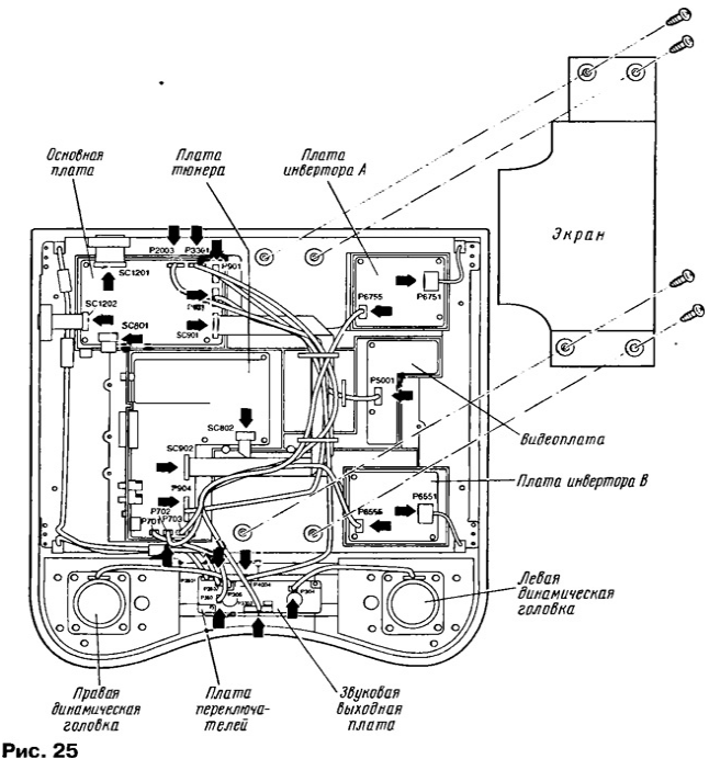
Values are set by the same VOLUME+ and VOLUME- buttons on the remote control. When repairing such TVs, you must be no less careful than when repairing conventional TVs. It is highly desirable to work in an antistatic wrist strap and on an electrically conductive mat, since all panels are "afraid" of electrostatic charges. Before proceeding with the repair, it is necessary to make sure that the parameters are set correctly as described above. For orientation during repair in Fig. 25 shows the placement of boards and other devices on the TV, as well as the location of the connectors. Wide black arrows on it show the directions for finding connectors to facilitate the removal and installation of boards.
Consider the possible malfunctions of the TV on specific examples. 1. There is no picture and sound. First of all, check the integrity of the fuses F2-F4 on the tuner board (see Fig. 14). If any of them (or several) has an open, then check the load circuits for a short circuit. When it is detected, first of all, the health of the power supply transformer T701 and transistors Q702, Q751, Q753 and the key element Q752 of the main board are checked (see Fig. 21, part 6). If there is no short circuit, check the presence of constant voltages at the outputs of the rectifiers and power supply stabilizers. In the absence of all supply voltages, the serviceability of the IC702 microcircuit, transistors Q702, Q703, as well as the absence of an open circuit in the fuses FB701, FB708, FB709 and the primary windings of the T701 transformer are checked. In the absence of any one supply voltage, the serviceability of the corresponding rectifier in the secondary circuits of the T701 transformer and the voltage stabilizer is checked. 2. No picture. They check the presence of digital video signals on the corresponding pins of the IC801 (see Fig. 17, part 3) and IC1201 (see Fig. 21, part 4) microcircuits of the main board. If their absence is found at the outputs of a particular microcircuit, then before replacing them (this is done as a last resort), the microcircuit mode is checked for direct current. It should not differ from that indicated on the circuit diagram by more than ±10%. Only after that they decide to replace the microcircuit or any of the elements surrounding it. If the necessary video signals are present at the outputs of the IC1201 chip and they are fed to the LCD panel, then first the signals and voltages on the IC1205 chip are checked, and then the serviceability of it itself, as well as the receipt of multiplexed signals on the panel. They also check the supply of the reference voltage REF from the IC1201 microcircuit (see Fig. 21, part 4) to the graduated voltage device (see Fig. 21, part 5), the serviceability of the IC1102-IC1108, IC1110 microcircuits included in it, and the presence of graduated voltages on the contacts panel connectors (see figure 21, part 4). In conclusion, the survey concludes that the panel itself is malfunctioning. 3. There is no image when a signal is applied to the antenna input. First, they check the presence of voltages of 5, 9, 12 and 31 V on the corresponding pins of the tuner connectors (see Fig. 14). It must be borne in mind that if the voltages of 5,12 and 31 V come from a power source located on the main board, then the voltage of 9 V is stabilized by the microcircuit 15 of the tuner board, which may fail. They also check other stabilizers - microcircuits BUT, I1 and transistors Q18 and Q28 located on the tuner board. Then, the presence of the CCVS video signal at the tuner output is checked. Its absence indicates a malfunction of the tuner. If there is a signal, it is necessary to trace (TV V circuit) whether it goes to the input (pin 3) of the IC402 chip (see Fig. 17, parts 1 and 3) and to its output (pin 7). If there is no signal at the output of the microcircuit, then either the microcircuit is faulty, or its control inputs (pins 2 and 4) do not receive the corresponding command signals (TV / AV and AV / IR) from the IC2001 control microcontroller (see Fig. 17, part 2 and 3). If there is a signal at the output of IC402, check the operation of the transistor Q420 of the main board (see Fig. 17, part 3) and the signal at pin 73 of IC801. If there is a signal, then the microcircuit is out of order. 4. There is no image when a signal is applied to one of the video inputs. With such a malfunction, three cases are possible. If there is no image when the S-VHS signal is applied (first case) to the SC5001 socket of the video card (see Fig. 18), check the passage of the brightness signal V1 SY - V1 V through the video card, the contacts of the P5001 / P903 connector, the IC402 chip (pins 1 and 7 ) and the transistor Q420 of the main board (see Fig. 17, parts 1 and 3) to pin 73 of the IC801 chip with the appropriate commands from the IC2001 control microcontroller (see above). As in the previous malfunction, if there is a signal, the microcircuit is defective. There may be no picture when a video signal is applied to pin 20 of the SCART connector (second case). They check the passage of the V2 V signal through the tuner board (see Fig. 14), the contacts of the SC902 / SC901 connectors, the Q421 transistor of the main board (see Fig. 17, part 3) to pin 74 of the IC801 microcircuit. If the signal comes, the microcircuit is faulty. And finally, if there is no image when a video signal is applied to the J5001 socket (third case) of the video card (see Fig. 18), check the passage of the V3 IN - SY OUT signal through the video card, pins of the P5001 / P903 connector (see Fig. 17, part 1 ), transistor Q820 of the main board (see Fig. 17, part 3) to pin 75 of IC801. If the signal is present, the chip is also faulty. 5. No sound in dynamic heads. They check the presence of signals 34 at the outputs (pins 12 and 8) of the IC3305 chip of the sound output board (see Fig. 16) and their flow through the contacts of the P304 and P305 connectors to the dynamic heads. If there are no signals, check the microcircuit mode for direct current and, first of all, the presence of a supply voltage of 13 V at its output 7. If the mode corresponds to that indicated in the diagram, check the receipt of 3H input signals to the microcircuit through pins 8 and 9 of the P3302 / P3301 connectors with the main boards (see fig. 21, part 6). It checks the health of the IC303, IC903 microcircuits (see Fig. 17, part 1) and the elements surrounding them, as well as the receipt of DACM R and DACM L signals from the IC901 processor (pins 27 and 28, respectively). And finally, they check the health of the IC901 processor itself, the elements surrounding it and the receipt of the MONOS sound signals (on pin 60) and SIF (on pin 67) from the tuner board at its inputs (see Fig. 14). The tuner itself may, of course, be faulty if both of these signals are absent. Additionally, they check the blocking voltage level at pin 53 of the IC2001 chip (see Figure 17, part 2), which should be low. Otherwise the sound will be blocked. 6. There is no sound in the headphones. The search for the cause of the malfunction begins with checking for the presence of audio signals at pins 24 and 25 of the IC901 processor on the main board (see Fig. 17, part 1). If they are not there, check the health of the processor and its surrounding elements. If the signals are present, first check the health of the IC304 chip and its surrounding elements, and then the passage of the HR and HL signals (see Fig. 17, parts 1 and 2) through the pins of the P2003 / P4004 connector to the J4001 headphone jack. It is located on the switch board (see fig. 15). 7. No audio signals on the line output. Check for 3H signals on pins 36 and 37 of the IC901 processor (see Fig. 17, part 1). If they are not, examine the processor and the elements surrounding it. If there are signals, check the health of the IC902 microcircuit and, if it and the elements surrounding it are working, the further passage of the V2R0, V2LO signals through the contacts of the SC901 / SC902 connector to the SCART connector of the tuner board (see Fig. 14). 8. No white balance. Depending on the color tone of the image, the range of the RO-R5 signals on pins 18-23 of the SC1201 connector (see Fig. 21, part 4) of the LCD panel, the GO-G5 signals on pins 25-30 and the BO-B5 signals on pins 32- 37. If there are no R signals or their range is significantly reduced, check the health of the resistors in the R1202, R1203 assemblies, if the G signals are in the R1204, R1205 assemblies, and if the B signals are in the R1206, R1207 assemblies. In the case when all the resistors are good, but some of the above signals are absent or they are small, pay attention to the mode of the IC1201 controller and then decide on its malfunction. 9. The backlight lamps do not light up. If all the lamps are not lit, it is most likely that the OFLO blocking command was sent to pins 2 of connectors R703 / P6755 and R702 / P6555 of the inverter boards (see Fig. 14 of the tuner board) through the connectors SC902 / SC901 from the output 34 of the IC1201 controller (see. Fig. 17, part 1 and Fig. 21, part 4), which stops the operation of both converters. In normal operating mode, the specified output of the controller should be a high voltage level. In this case, the key element Q3603, located on the main board, may also be faulty. But the most likely malfunction is when three backlight lamps do not light up. In this case, first check the integrity of the fuses F1 and F5 on the tuner board (see Fig. 14), through which the 13 V supply voltage passes to the inverter boards. If the fuses are intact, they check the operability of the corresponding voltage converter (see Fig. 19), that is, the serviceability of its elements, primarily transistors and transformers. If only one lamp does not light up, then either it is faulty, or one of the windings of the corresponding transformer in the converters is cut off. Literature
Author: A. Peskin, Moscow
Alcohol content of warm beer
07.05.2024 Major risk factor for gambling addiction
07.05.2024 Traffic noise delays the growth of chicks
06.05.2024
▪ Data storage time in SSD increased thousands of times
▪ section of the site Power supply. Article selection ▪ article Psychology of development and developmental psychology. Lecture notes ▪ article What animal scored on an IQ test at a normal adult American level? Detailed answer ▪ article Locksmith-grinder. Standard instruction on labor protection ▪ article Speeding up a reaction - how catalysts work. Chemical experience
Comments on the article: Alexander Thanks to the author for the excellent presentation of such a complex material. I wish you further, difficult creative popularization of modern television. [up]
Home page | Library | Articles | Website map | Site Reviews
www.diagram.com.ua |


 Leave your comment on this article: