|
|


 Arabic
 Bengali
 Chinese
 English
 French
 German
 Hebrew
 Hindi
Hindi Italian
 Japanese
 Korean
 Malay
Malay Polish
 Portuguese
 Spanish
 Turkish
 Ukrainian
 Vietnamese
|
ENCYCLOPEDIA OF RADIO ELECTRONICS AND ELECTRICAL ENGINEERING Highly sensitive DMB converter. Encyclopedia of radio electronics and electrical engineering
Encyclopedia of radio electronics and electrical engineering / Телевидение The converter proposed for repetition converts the signals of the 21st - 39th television channels of decimeter waves (UHF) into oscillations of any of the twelve channels of meter waves (MB). It has high sensitivity, selectivity and high gain. Technical specifications The schematic diagram of the converter is shown in the figure. The signal coming from the UHF receiving antenna via a coaxial cable with a wave impedance of 75 ohms enters the input circuit L1C1 with a quality factor. equal to about 25 (bandwidth - about 25 MHz). The choice of a relatively high value of the quality factor is due to the need to increase the sensitivity of the converter and increase the immunity from interference due to crosstalk when receiving powerful interfering signals. A further increase in the quality factor by reducing the switching coefficients of the antenna and the radio frequency amplifier (URCH) in the L1C1 circuit leads to excessive sharpness of tuning to the channel by the capacitor C1 and a decrease in the efficiency of the input circuit.
URC converter - cascode, on transistors VT1, VT2. Its load is the circuit L2C5. Through the capacitor C6, the signal passes to the emitter of the transistor VT3 of the frequency converter. By appropriately connecting the cascades to line 1.2, the output (URCH) and input (converter) resistances are matched at the selected quality factor of the circuit. The local oscillator voltage is taken to the base of the converter transistor VT3 from part of the L3 line. It forms with capacitor C9 a local oscillator circuit made on a transistor VT4 according to a capacitive three-point circuit. The coefficient of inclusion of the transistor in the circuit is determined by the ratio of the capacitance of the capacitor C11 and the capacitance of the emitter junction Ce. By changing the capacitance of the VDI diode connected to the circuit through capacitors C8 and C 12, you can smoothly adjust the local oscillator within one channel. For this, a closing voltage is applied to the diode, which is regulated by a variable resistor R10. Resistor R7 prevents the occurrence of throttling self-oscillations. An increase in the sensitivity of the converter compared to similar devices was achieved by choosing the optimal operating mode for the VT1 transistor in terms of noise figure and using a stabilized bipolar supply voltage source. Such a power supply made it possible to create a common base mode for the converter transistors for direct current, that is, to connect the bases directly to a common wire and dispense with dividers in their circuits and blocking capacitors for alternating current. This helped to get rid of the high-frequency capacitance flickering noise inherent in the latter, to reduce the number of parts and, consequently, the parasitic capacitances and inductances caused by them. The absence of a blocking capacitor in the base circuit of the VT4 transistor of the local oscillator made it possible to obtain a higher purity of the spectrum of generated oscillations [1]. In addition, the use of a bipolar power supply completely solved the problem of thermal stabilization of the cascades. The noise of the transistor VT1 depends both on the DC mode and on matching the input of the UFC. Measurements have shown [2] that the noise factor of the cascade on a bipolar transistor is practically independent of the collector-emitter voltage and increases only at its low values (less than 3 V). Its dependence on the collector current for most modern microwave transistors has a weakly pronounced minimum at values of 1...5 mA. The most significant factor in increasing the sensitivity of the converter is the provision of the so-called optimal mismatch mode at the input of the URF, in which the noise figure of the stage is reduced to a minimum value. The calculation of such a mode is simple, but it assumes the presence of mode-frequency dependences of the Y-parameters of the transistor used, which are not always available for radio amateurs. Therefore, if other transistors are supposed to be used instead of those indicated in the diagram, you can proceed as follows. Since the active component of the input conductivity of the transistor depends on the collector current, the maximum sensitivity of the converter can be achieved by changing it within 1 ... 10 mA. Although in this case the collector current is unlikely to correspond to the minimum intrinsic noise of the transistor, the loss in noise figure after careful tuning, even in the worst case, will not exceed 0,5 dB compared to the minimum achievable [3]. Details. The converter uses constant MLT resistors (R1-R3 - group A, i.e. with a normalized noise voltage of not more than 1 μV / V). Variable resistor R10 - any, with a resistance of 47 ... 100 kOhm. Trimmer capacitors C1, C5, C9 - KPK-MP, through passage C4 - KTP or any suitable in size with a capacity of 180 ... 4700 pF, the rest, except for SI, - KM, KD with a capacity of 100 ... 620 pF. It should be noted that the radial and axial play of the rotors in trimmer capacitors is unacceptable. Capacitor C11 (1pF) - a piece of a 75-ohm cable with fluoroplastic insulation (capacitance per unit length 0,55 ... 0,67 pF / cm) about 20 mm long (specify when setting up, starting from 35 mm). Choke L4 is wound in bulk on a paper frame with a diameter of 3 mm and contains 100 turns of PEV-2 0,1 wire (winding length - 5 mm). Instead of the KD503A diode, you can use KD509A. KD510A or KD521, KD522 with any letter index, instead of transistors KT3128A - GT330Zh, KT3127A, KT371A, any of the series KT382, GT329, GT383, KT372A, KT3120A, KT3123A (named in the order in the manner converter parameters). When using npn structure transistors, it is necessary to change the polarity of the VD3101 diode and power supplies.
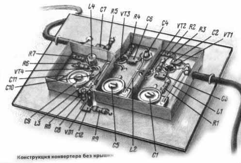
The design of the converter is shown in Fig.2. Its installation is volume-printed, using a board, the drawing of which is shown in Fig. 3. It is made of double-sided foil fiberglass with a thickness of 1,5 mm. Since in the UHF range the depth of penetration of high-frequency currents into copper printed conductors does not exceed a few micrometers, in order to reduce high-frequency losses in the metal and increase the quality factor of the oscillatory circuits, the surface roughness of the board on the mounting side should be as small as possible. To do this, it is polished to a mirror finish with grinding micropowders, GOI paste or toothpaste and covered with a thin layer of any nitro-lacquer diluted with acetone in a ratio of 1: 2. This treatment will prevent the oxidation of the copper surface layer and maintain its high electrical conductivity for a long time. During installation, the foil in the places of soldering parts is cleaned of varnish with the sharp end of a knife. Since the conductivity of the solder is about an order of magnitude worse than the conductivity of copper, it is not recommended to treat large areas of the foil, the amount of solder at the soldering points should be as small as possible. The conclusions of the elements should be as short as possible; for separating and blocking capacitors, they are soldered completely, having previously cleaned the soldering points from paint. Transistors are rigidly inserted into the holes intended for them (when using other transistors, these holes may not be needed at all). To reduce the influence of the screwdriver used on the tuning frequency of the circuits, the terminals of the rotors of the tuning capacitors C1, C5, C9 are soldered to the board (common wire), the stator petals are bitten off. The component lead connections (two, three, or four) shown in the drawing without solder points are located above the board. The dots indicate the places of soldering to the foil on the corresponding side of the board. Lines L1-L3 are pieces of uninsulated polished copper wire with a diameter of 1 mm and a length of 22 (L1, L2) and 24 (L3) mm. One end of the wire of each line is soldered to the output of the stator of the trimmer capacitor, the other to the common wire, bent along a radius of 7 mm (LI, L3), or to the output of the feedthrough capacitor C4 (L2). The segments are placed above the board at a height of 5 mm for the 21st - 35th channels and 3 mm for the 36th - 39th channels. The distances to the soldering points of the elements (counting from the ends connected to the common wire directly or through the capacitor C4) for L1 are 4,3 and 5.5 mm, for L2 - 3,5 and 12 mm. at L3 - 4 mm. To shield the converter stages, walls and partitions 12 mm high made of copper or brass 0,3 ... 0,5 mm thick with cutouts and holes for the leads of the elements are soldered to the board. It is not necessary to shield the converter output circuit. After the installation is established, the installation is closed from above with a lid of the same material with holes for access to the rotors of capacitors C1, C5, C9. In order to increase the mechanical strength, the antenna and output cables are fixed to the board with wire brackets. Setting up the converter begins with checking the current consumption, which should be approximately 10 mA. For power supply at this stage, it is desirable to use galvanic cells, which will avoid the possible influence of ripple and interference from the stabilizer. Then they make sure that the local oscillator is working, for which they connect the output of the converter to the input of the TV, which is connected to a free channel. When the local oscillator is working properly, supplying power to the converter leads to an increase in sound noise, and the rotation of the rotor of the capacitor C9 changes their intensity and flashes on the TV screen. If this does not happen, a piece of coaxial cable 11 mm long is included as a capacitor C35. The desired result is achieved by gradually shortening it with a sharp knife (if the cable diameter is less than 3 mm, it is necessary to ensure that after trimming the braid is not connected to the central conductor). In case of failure, the described procedure is repeated with an increased emitter current of the transistor VT4, for which the resistance of the resistor R6 is reduced to 1.5 kOhm. Having achieved stable operation of the local oscillator, tune it to the desired frequency. To do this, the antenna cable is connected to the left (according to the diagram) plate of the capacitor C6, having previously unsoldered it from the L2 line. By rotating the rotor of the capacitor C9, at least a faint image appears on the TV screen when received in the selected MB channel. Having restored the connection of the capacitor C6 with the line L2, connect the antenna cable through a capacitor with a capacity of 10 ... 30 pF to the emitter of the transistor VT2 and, rotating the rotor of the capacitor C5, adjust the URF circuit according to the best image on the screen. If there are no resonant phenomena, that is, the position of the rotor of the capacitor C5 does not affect the image quality, then the inductance of the line L2 is corrected by changing the height of its location above the board. Then a signal is applied to the input of the converter and the input circuit L1C1 is adjusted in the same way. Further, instead of resistor R2, a constant resistor with a resistance of 820 ohms and a variable with a resistance of 10 kOhm are connected in series. By changing the last emitter current of the transistor VT1 and adjusting the input circuit, they achieve the maximum sensitivity of the converter for the highest image quality. After measuring the impedance of the resistors in the emitter circuit, replace them with one resistor with the closest rating. Meteorological conditions greatly affect the distribution of DMV. Therefore, in an area located in the zone of uncertain reception, it is advisable to select the mode of the transistor VT1 for the best sensitivity in steady weather a few hours before or after sunset. In conclusion, close the converter with a lid, solder it along the perimeter to the walls of the screen, and finally adjust the contours of L1C1 and L2C5 through the holes in it. It should be remembered that adjustment of the input circuit is sometimes necessary when changing the length of the antenna feeder, the location of the antenna, or replacing it with another one. Literature
Author: M.Zaitsev, Elektrostal, Moscow Region; Publication: N. Bolshakov, rf.atnn.ru
Energy from space for Starship
08.05.2024 New method for creating powerful batteries
08.05.2024 Alcohol content of warm beer
07.05.2024
▪ Supersonic biplanes are more economical than conventional aircraft ▪ Created an artificial nerve to combat chronic pain ▪ Cooler Thermaltake ToughAir 510
▪ section of the site Interesting facts. Selection of articles ▪ article Either in the snout or the pen, please. Popular expression ▪ article Can animals distinguish colors? Detailed answer ▪ article Work on phototypesetting equipment. Standard instruction on labor protection ▪ article Mixer. Encyclopedia of radio electronics and electrical engineering
Home page | Library | Articles | Website map | Site Reviews
www.diagram.com.ua |


 Leave your comment on this article: