|
|


 Arabic
 Bengali
 Chinese
 English
 French
 German
 Hebrew
 Hindi
Hindi Italian
 Japanese
 Korean
 Malay
Malay Polish
 Portuguese
 Spanish
 Turkish
 Ukrainian
 Vietnamese
|
ENCYCLOPEDIA OF RADIO ELECTRONICS AND ELECTRICAL ENGINEERING Power amplifier KB radio station. Encyclopedia of radio electronics and electrical engineering
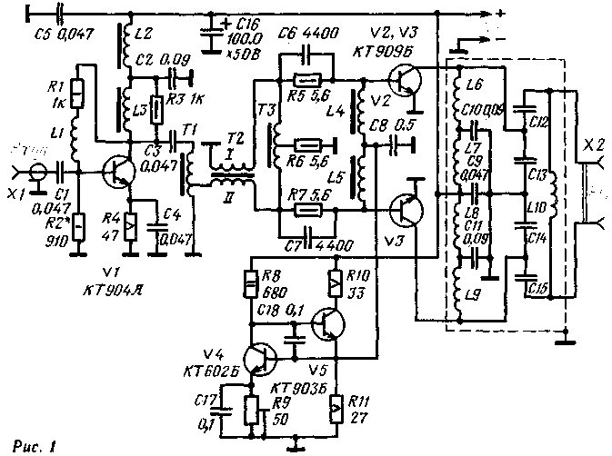
Encyclopedia of radio electronics and electrical engineering / RF power amplifiers The amplifier is designed to amplify SSB and telegraph signals on amateur KB radio stations of the first category. The power supplied to the final stage of the amplifier is 200 watts. overall efficiency in single-tone signal mode - no worse than 55%, power gain - no less than 40 dB, intermodulation distortion - no worse than -28 dB, the level of harmonic components of the output signal does not exceed -55 dB. The amplifier has a balanced output, the output impedance is 75 ohms. With some complication of the output device, it can also be used with an asymmetric load. To power the amplifier, a stabilized voltage source of +30 V with a current of up to 7-8 A is required. The preliminary stage of the amplifier (Fig. 1) is broadband. It is assembled on transistor V1, which operates in class A mode. The bias based on transistor V1 is created by a voltage divider formed by resistors R1 and R2. Coil L1 serves to equalize the gain of the cascade at different frequencies.
The output stage is push-pull, on transistors V2, V3. For maximum suppression of the most powerful second harmonic, as well as the remaining even harmonics, the output stage transistors should be selected with approximately the same transfer coefficient values. The required excitation power of the output stage is 1,4 W. To coordinate the preliminary stage with the final stage, an autotransformer T1 is used, which has a transformation ratio of 3. The phase opposition of the voltages exciting the output transistors is ensured by balancing transformers T2, T3. The power of the even harmonic components of the signal and the proportion of odd harmonics, which is associated with the deviation of the phase difference of the voltages at the output of the balun from 180°, is dissipated by the resistor R6. Chains C6R5 and C7R7 stabilize the operation of the amplifier and protect the base circuits of the output stage transistors from overload. In addition, the C6R5 and C7R7 chains even out the gain of the final stage at higher frequencies. The connection of the amplifier with the output resonant circuit L10C12-C15 is capacitive. Parallel power is used in both stages of the amplifier. There are decoupling LC filters in the power circuits, and the bias voltage to the bases of the transistors of the final stage is supplied through the chokes L4 and L5. On transistors V4 and V5, a device is assembled that allows you to get a "floating", that is, depending on the level of the input signals, the bias current. The device is a push-pull DC amplifier covered by 9% negative feedback. As a result of such feedback, the output dynamic resistance is very small, which provides the desired changes in the instantaneous values of the base currents at the smallest potential changes. The initial current is set by resistor RXNUMX. The details of the resonant circuit L10C12-C15 for the midpoints of the amateur bands selected by the author (3,575; 7,050; 14.175; 21.225 and 28,850 MHz) are given in Table. 1. The L10 coil is wound with PEV-1 2,26 wire without a frame.
If it becomes necessary to operate the amplifier for an unbalanced load, the final stage circuit should be changed as shown in Fig. 2.
In this case, the broadband transformers T4 and T5 allow you to switch from the balanced output of the final stage to the unbalanced P-loop C21L11C22. The parameters of the latter are given in Table. 2 (the wire and winding method of the coil of L11 are the same as those of L10). The quality of the amplifier is largely determined by the thoroughness of the manufacture of transformers. All of them are wound on ring magnetic cores made of 100NN ferrite: T1-TZ of size K20X12X6, the rest - K32X12x6. The T4 transformer uses two rings stacked together, and the T5 uses three. In the absence of recommended transformers, they can be made on magnetic circuits with higher magnetic permeability, but this will reduce the output power at high frequency ranges.
The windings of the transformers are made with several PEV-1 0,47 wires slightly twisted and connected in parallel. Transformer T1 has three windings connected in series (the end of the first - with the beginning of the second, etc.). Each winding consists of seven turns and is made in three wires. Retraction - from the 7th turn from the bottom according to the scheme. Transformers T2 and T3 consist of two windings in three wires. The number of turns in the windings is 10 each. They are wound with six wires at the same time. The windings of the transformer T3 are connected in series, the point of their connection is connected to the resistor R6. The T4 transformer has two windings of eight turns in five wires (the winding is carried out with ten wires at the same time). The connection scheme is similar to T3. The T5 transformer contains two windings of eight turns in eight wires (winding-16 wires at the same time). The L1 coil is wound with PEV-1 0,3 wire on a frame with a diameter of 11 mm, the winding length is 22 mm, the number of turns is 30. Chokes L2-L6 are made on K20X12X6 magnetic cores made of ferrite 1000NM (L2) and 100NN (the rest). L2-L3 contain 30 each, L4 and L5 each contain 16 turns of PEV-1 1,12 wire. Inductors L.6-L9 are wound on frames with a diameter of 22 mm, the winding length is 30 mm, the number of turns is 25, the wire is PEV-1 0,38. Resistors MLT or VS (R9-YUS), capacitors KD, KM-5, KSO-1 can be used in the amplifier. KSO-5 (C16-K50-6). Capacitors C2, C10 and C11 consist of two 0,047 uF capacitors connected in parallel, C6 and C7 - of two 2200 pF capacitors, C8 - of five 0,1 uF capacitors, C19 and C20 - of six 0,047 pF capacitors . The reactive power that capacitors C12-C15 and C21, C22 can withstand must be at least 80 V-A (several KSO capacitors can be connected in parallel). The requirements for the design of the amplifier are common for such equipment (the shortest length of the connecting wires, especially in the circuits of the bases of the transistors V2 and V3 and the capacitors of the decoupling filters). The input and output elements of the push-pull cascade must be placed symmetrically, the elements of the matching circuit must be shielded. The body of the amplifier is made of brass 6 mm thick, it serves as a heat sink for transistors V1-V3. It is very important to ensure good thermal contact between the transistors and the case. For this, the places of their contact are ground and coated with a non-drying lubricant. Before proceeding with the adjustment of the amplifier, it is necessary to check the correct installation. After making sure that there are no errors, only the cascade on transistor V1 is connected to the power source. The current of the transistor is selected with the resistor R2 so that the voltage drop across the resistor R4 is 11 V. Connect the supply voltage only to the output stage and the "floating" bias device. Set (resistor R9) the output stage current to 0,3 A. Having restored the connections and connected the equivalent of the antenna to the output (a resistor with a resistance of 75 ohms and a power of 100 W), turn on the amplifier at a supply voltage of 15 V. Now you need to be extremely careful, since the transistors can fail as a result of the slightest excess of the maximum allowable dissipation power, collector current, collector-emitter voltage (for example, when the amplifier is self-excited), reverse voltage at the emitter junction, etc. Make sure that there is no self-excitation (using an RF voltmeter) and gradually increase the supply voltage to 30 V. Having applied an exciting RF voltage to the input of the amplifier, the resonant circuits are tuned by changing the length of the winding. With an input voltage of 0,3-0,6 V, the output voltage should be 57 V, and the output stage current should be 6,7 A. Having previously well coordinated the antenna with the feeder, connect it to the amplifier. They control the voltage on transistors V2, V3 and the current of the output stage. Increase the input voltage until the output becomes equal to 57 V. The output current should be equal to 6,7 A. A lower current value will indicate poor matching of the amplifier with the load. After adjustment, the amplifier can be connected to the exciter with a short piece of cable (10-15 cm). If the length of this cable is longer. it is necessary to match the input impedance of the amplifier (16-18 ohms) with the cable resistance using a broadband transformer on a ferrite ring. Author: M. Bakhmetov, Nizhyn, Chernihiv region; Publication: N. Bolshakov, rf.atnn.ru
Artificial leather for touch emulation
15.04.2024 Petgugu Global cat litter
15.04.2024 The attractiveness of caring men
14.04.2024
▪ Absolutely unbreakable screen for gadgets ▪ To like people, you need to train the brain ▪ Analog to Digital Converter LTC2255 ▪ U-shaped photoelectric sensors of the BUP series from Autonics
▪ section of the website Electrotechnical materials. Article selection ▪ article Europe can wait. Popular expression ▪ article Vetvyanka is stupid. Legends, cultivation, methods of application ▪ article Stable coin. Focus Secret
Comments on the article: de UU4JGC Yuri What about lightning protection?
Home page | Library | Articles | Website map | Site Reviews
www.diagram.com.ua | |||||||||||||||||||||||||||||||||||||||||||||||||||||||||||||


 Leave your comment on this article: