|
|


 Arabic
 Bengali
 Chinese
 English
 French
 German
 Hebrew
 Hindi
Hindi Italian
 Japanese
 Korean
 Malay
Malay Polish
 Portuguese
 Spanish
 Turkish
 Ukrainian
 Vietnamese
|
ENCYCLOPEDIA OF RADIO ELECTRONICS AND ELECTRICAL ENGINEERING UHF amplifier from SK-D-1. Encyclopedia of radio electronics and electrical engineering
Encyclopedia of radio electronics and electrical engineering / Телевидение Recently, there are more and more TV stations operating in the UHF bands. Their power is relatively small, and therefore the reception of such stations is very difficult. In many cases, the installation of UHF amplifiers helps. A broadband amplifier does not always help out, especially if a powerful transmitter is working nearby, and you are "hunting" for a remote TV station. And to assemble and configure such an amplifier is far from easy. Everyone who has ever tried to make such a device knows that the result does not always live up to expectations. Obviously, in this case it is best to use an amplifier with a frequency response that can be tuned to the desired range. The use of such an amplifier can significantly improve the reception of UHF stations due to the high selectivity of the cascades. However, the construction of such an amplifier can only be done by very experienced radio amateurs who have the opportunity to use the necessary measuring instruments. But what about those radio amateurs who cannot purchase the necessary parts, do not have the necessary measuring instruments? Nevertheless, the way out in this situation is simple - it is the use of ready-made industrial units available to radio amateurs. The SK-D-1 block, which was used in tube-semiconductor TVs, was taken as the basis. Its simple alteration, which even a novice radio amateur can perform, allows you to get a UHF amplifier with good performance. Operational characteristics of the UHF:
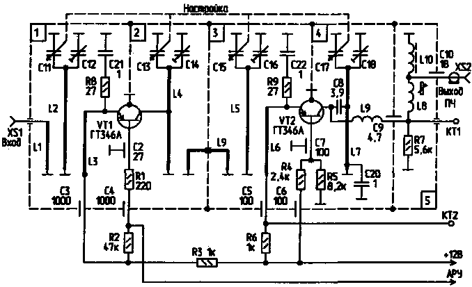
The advantages of such an amplifier include high selectivity and significant interference suppression on adjacent channels. There is also a drawback - the need for restructuring (by rotating the rotor knob) when switching to another channel. However, if reception is carried out on one UHF channel, there is no need for restructuring. Figure 1 shows the original diagram of the SK-D-1 block, and Fig. 2 shows the diagram of the SK-D-1 after alteration, i.e. circuit diagram of the amplifier itself.
Consider the original block diagram SK-D-1 (Fig. 1). In the first chamber there is a cascade on the transistor VT1 (circuit with OB). Resonator L1 provides input matching with the antenna, L2 with capacitances SI and C12 form a tunable input circuit for tuning to the desired channel. The collector of the transistor VT1 is loaded on the circuit L4-C13-C14, which is located in the second chamber. Further, the signal passes to the circuit L5-C15-C16, located in the third chamber. Through the inductance L6, the signal enters the emitter of the transistor VT2. On the transistor VT2, a converter of the RF signal to the IF of the TV is assembled. Transistor VT2 is connected according to the capacitive three-point circuit, the load of the cascade is L9, which, together with C17, C18, C8, L7, C20, is located in the fourth chamber.
Alteration SK-D-1 is as follows: - since under normal operating conditions the first stage on the transistor VT1 is controlled by the AGC system of the television receiver, it is necessary to set the operating mode without AGC; - transfer the second stage on the transistor VT2 from the conversion mode to the amplification mode. When getting started, remember that you need to handle the unit carefully, because. the slightest changes in the arrangement of parts with careless disassembly can cause detuning of circuits with resonant circuits. So, having removed the spring bar at the top of the cover, carefully remove the cover itself. The number of cameras (there are only 5 of them) is counted starting from the antenna input socket. Carefully inspect the interior installation. There should be no obvious damage inside - burnt and broken resistors, capacitors. When the handle of the vernier mechanism is rotated, the movement of the plates of the quadruple capacitor must be free, without closing the plates between themselves or with other elements. When working with the block, it is impossible to change the position of the trimmer capacitors, made in the form of silver-plated plates and located in front of the sections of the variable capacitor, as well as resonant lines, made in the form of silver-plated tires and wire segments. Solder the following items carefully: - C8, C20, L9 located in the 4th chamber; - L8, L10 and R7 located in the 5th chamber. Resistor R7 may be missing in some instances of SK-D-1. Next, you need to determine the brand of transistors that are available in this block SK-D-1. The fact is that instead of the transistors indicated in the diagram (Fig. 1), there may be others, for example, AF-239 and AF-139, which are analogues of the GT346A and GT346B transistors, respectively. If a GT2B or AF-346 transistor is installed as VT139, it will have to be removed and replaced with GT346A. Transistors of this type are used in almost all SK-D units, as well as in SK-M units with electronic tuning, so, in principle, it is not difficult to find such a transistor. Before installing a new transistor, it should be checked. If the test will be carried out with an ohmmeter, it should be remembered that the supply voltage of the ohmmeter may exceed the allowable reverse voltage of the emitter junction. Therefore, when determining the health of the transistor with an ohmmeter, you should not use the low-resistance limits of the ohmmeter. If there is a choice of several transistors, you should choose a transistor with the largest possible value of h21e. Before installing the transistor, it is necessary to connect its common terminal ("body") by soldering to the body of the transistor itself. Above the window of the chamber in which the transistor is located, there may be a piece of thin silver-plated wire. This segment is the "tail" of L6. Therefore, in no case do not try to remove it by soldering. Due to heating, the position of L6 in space may change, which will lead to a detuning of the circuit. You need to remove the "tail" with side cutters. The case output of the transistor VT2 should be inserted into a small hole, which is under the resistor R8, and soldered from the side of the 4th chamber. The collector output should be soldered to the same point on L7 where the output of the removed transistor was soldered. Carefully solder the emitter and base leads without overheating the solder points, as the solder points are low-capacitance capacitors that can be destroyed if overheated. Next, you need to remove the resistors R6 and R4, thus disconnecting the second stage from the power circuits. Then it is necessary to install the resistors Rd1, Rd2 and RdZ, as shown in Fig. 3. Set the slider of the resistor Rd2 to the middle position. By applying a voltage of +12 V to the circuit, by rotating the slider of the resistor Rd2, set the voltage to +9,5 V at the emitter and +9 V at the base of the transistor VT1. Then, turning off the power, measure the total resistance of the resistors Rd2 and Rd3. Select an MLT-0,125 type resistor with a value close to the measured one and install it in the circuit (R10 in Fig. 2), Rd1 will remain in the circuit as R11. Reapply power to the circuit and check the voltage at the terminals of the transistor VT1.
The operation of the first stage can be checked visually, according to the image on the TV screen. To do this, tune the TV to one of the UHF channels, which is received with poor quality. Then, disconnecting the antenna cable from the TV input, connect it to the input of the amplifier. A piece of cable RK-75 with a plug soldered at one end is connected to the UHF input of the TV. The braid of the other end of the cable is soldered to the amplifier case, and the central core is soldered through a capacitor with a capacity of 4,7 pF to the soldering point of the collector output of the transistor VT1. Although the peak point of the signal is on L4 closer to the case, you should not solder in places where there is no factory soldering, in order to avoid deterioration of the circuit parameters. Turning on the power of the amplifier, by smooth rotation of the vernier mechanism, tune it until an image is obtained on the screen. The image should be of better quality compared to what it was before connecting the unit. Then check the operation of the circuit L5-C15-C16. To do this, turning off the power and unsoldering the cable from L4, solder it to the junction of L5 and C15. Turn on the amplifier power again and monitor the signal for image quality. In this case, there should be no deterioration in image quality. The setting of the second stage is similar. After turning off the power to the amplifier, the resistor R6 is soldered in place (Fig. 2), and instead of the removed resistor R4, a tuning resistor is installed, with a nominal value of 5,1 ... 10 kOhm, and its engine is set to the middle position. Then the "control" cable is soldered through a capacitance of 4,7 pF to the soldering point of the collector of the transistor VT2 and the power is turned on. By smoothly rotating the resistor slider, the modes of the transistor VT2 are set with the same values as those of VT1. Then the power is removed, the resistance of the variable resistor is measured and the MLT resistor with a value close to the measured one is soldered instead. In conclusion, the socket KT1 and the passage capacitor C9 are removed. The RK-75 cable is inserted into the holes formed, which will be connected to the TV. The cable sheath is soldered to the "case", and the central core - through the capacitor C22 to L7, selecting the soldering point experimentally, according to the best image quality. The amplifier can be enclosed in any suitable decorative case. If the amplifier will be used on several channels, then it is convenient to mark the desired channels on the case, and at risk on the tuning knob. And in conclusion about further improvement. The author does not consider it expedient to increase the sensitivity to include broadband amplifiers before the input of the device, since due to the uneven frequency response and the high noise level of such devices, the reception quality on high-frequency channels can sharply decrease. Good results can be obtained by switching on a one- or two-stage broadband amplifier after the output of this amplifier. In this case, you will have to carefully match the input and output of both amplifiers. Author: V. Sinitsky, Pervomaisk, Nizhny Novgorod region; Publication: N. Bolshakov, rf.atnn.ru
Alcohol content of warm beer
07.05.2024 Major risk factor for gambling addiction
07.05.2024 Traffic noise delays the growth of chicks
06.05.2024
▪ The growth of the smart toy market ▪ Charging station Bluetti AC180
▪ section of the site Grounding and grounding. Selection of articles ▪ You can lean on bayonets, but you can't sit on them. Popular expression ▪ article Sailing catamaran. Personal transport ▪ article Double balanced mixer SA612A. Encyclopedia of radio electronics and electrical engineering
Home page | Library | Articles | Website map | Site Reviews
www.diagram.com.ua |


 Leave your comment on this article: