Chips KR1008VZH18 and KR1008VZH19. Encyclopedia of radio electronics and electrical engineering

Encyclopedia of radio electronics and electrical engineering / Telephony
 Comments on the article
IS KR1008VZH18 (similar to SAMSUNG - KT3170, MITEL - MT8870, HUALON - HM9270) and KR1008VZH19 (similar to UMC - UM91531) is manufactured by NPO "INTEGRAL" in Minsk.
IS KR1008VZH19 is a tone-pulse (DTMF/PULSE) dialer with parallel input of information. Operates under the control of a microcontroller (computer) and generates both DTMF and pulse dialing signals. The frequencies of all necessary two-tone and pulse signals are generated by a crystal oscillator. IP is applicable in telephone, facsimile and modem communication equipment, remote control systems.

Main characteristics of IS KR1008VZH19
Parallel input of 4-digit information from the microcontroller (computer).
The inputs and outputs of the TTL chip are compatible.
To ensure high accuracy and frequency stability, a crystal oscillator with a frequency of 3,579545 MHz is used.
Supply voltage 2,5 - 5,5 V.
Possibility to select the impulse coefficient.
The dialing pulse frequency is 10 Hz.
Tone (DTMF) transmission of digits 0 - 9, *, #, A, B, C, D.
Pulse (PULSE) transmission of digits 0 - 9, *, #, A.
High tone output level: 2 dB.
Small non-linear distortion of the DTMF signal.
Compatible with RS-470 interface and CERT.
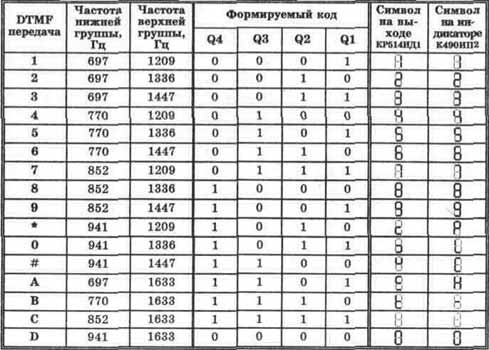
The IC pinout is shown in fig. 8.1, assignment of conclusions in table. 8.1, block diagram in fig. 8.2. Timing diagrams of inputs and outputs of IS KR1008VZH19 are shown in fig. 8.3, static and dynamic characteristics in table. 8.2 and 8.3. The output signals DTMF and PULSE of the IC KR1008VZH19, corresponding to the parallel code at the inputs D0 - D3, are given in Table. 8.4.

(click to enlarge)
Tab. 8.1. Assignment of the conclusions of the IS KR1008VZH19.
| Hack and predictor Aviator |
designation |
appointment |
| 1 |
FASHION |
Tone (DTMF) transmission mode selection input. With a "high" level at this input, the operation of the TONE and ACK outputs is normal (see the assignment of pins 14 and 16). When DTMF is "low", the TONE output is generated continuously and any new data on the 4-bit parallel input DO + D3 is ignored. This input is only active when the IC is in DTMF signal mode (T/P input is "low" level). |
| 2 |
LATCH |
Download input. When the input signal at this input goes from "low" to "high" (on a rising edge), the IC loads data on the 4-bit data input D0 - D3 and the T/P' input (pin 4). Dialing starts when the level at the LATCH input changes from "high" to "low". The signal level at the LATCH input must not change from "low" to "high" again, and new data cannot be loaded while the level at the ACK output (pin 14) remains "low". |
| 3 |
M / S |
Pulse factor selection input. "High" level at this input sets the pulse factor 1,5, "low" - 2 (the input must be connected either to the power plus or to the common output). Changing the state of this pin when the CE chip sample input (pin 13) is in the active ("low" state) enables the test mode. |
| 4 |
T/R |
Transmission method selection input (DTMF or PULSE). The input sets which of the modes - tone ("low" level) or pulse ("high" level) will be active. It is loaded along with a 4-bit data code on inputs D0 - D3. |
| 5 6 7 8 |
D0 Dl D2 D3 |
4-bit data input. This 4-bit parallel input is used to receive data from the microcontroller. (The diagram of input and output signals is shown in Fig. 8.3). The input data on these inputs must be applied before or during the rising edge of the "load" signal. |
| 9 |
DP |
Pulse key output. The output is made on an n-channel open-drain CMOS transistor. During dialing, the line break pulses are closed by a key to a common wire. In all other cases, the key is closed. The dialing frequency is 10 Hz, and the inter-series pause is 823 ms. (The status of this output in test mode is described below.) |
| 10 |
OV |
Common output (minus power). |
| 11 |
OSC0 |
generator output. |
| Hack and predictor Aviator |
designation |
appointment |
| 12 |
OSC1 |
Generator input. The IC contains an oscillator with the necessary decoupling capacitors and a feedback resistor in its package. Therefore, for the generator to work, it is enough to connect a standard television quartz at a frequency of 3,579545 MHz to the OSCO and OSC1 pins. (Practice has shown that in some cases the IC generator KR1008VZH19 does not start without capacitors with a capacity of 30 pF connected from the OSCO and OSC1 terminals to a common wire). You can also apply an external clock directly to the OSC1 pin. Generator operation is only possible with a "low" level at the CE input. |
| 13 |
CS |
Crystal sampling input. The input controls the start of the generator and is used for the initial setting of the microcircuit. "Low" level allows the operation of the microcircuit, "high" - prohibits. |
| 14 |
ASA |
Exit "confirmation". Generates a "confirmation" signal for the microcontroller. When the IC is ready to dial the next digit, the ACK output goes "high". It becomes "low" immediately after the rising edge of the "load" signal passes and remains in this state until the input data register is released (Fig. 8.2), i.e., the set of the loaded digit is completed. |
| 15 |
tons |
Tone output (DTMF) signal. It consists of an n-p-n transistor, the collector of which is connected inside the IC to the power plus, and the emitter is the output of the DTMF signal. The generated DTMF signal inside the IC is fed to the base of this transistor, which is connected according to the emitter follower circuit with a resistor installed between the IC output and the common wire. From the resistor, the signal is fed to an external amplifier on a transistor with a common collector, or connected according to the Darlington circuit. The duration of the DTMF signal is 70 ms, the inter-digit interval is 70 ms. The typical output impedance of a DTMF signal is 1,25 kΩ. The static current transfer coefficient (h21e) of the npn transistor is at least 30 at the collector current (Ik) = 3 mA. |
| 16 |
UDD |
Supply voltage (2,5...5,5 V). (Plus food). |
Maximum permissible characteristics of IS KR1008VZH19:
- Supply voltage (OV + UDD) .................................. -0.3 V to +10 V.
- Input voltage (Uin) .................................. -0,3 V to (UDD + 0,3, XNUMX) V.
- Permissible power dissipation (at 25 C) .............................. 600 mW.
- Operating temperature (Thor) ................................................ from - 20 C to +70 C.
- Storage temperature (ТstG) ......................... from -55 C to +125 ° C.
Operation of the IC in extreme conditions is not recommended. Exceeding them causes damage to the microcircuit. For reliable operation of the IS, it is recommended to be guided by the static and dynamic characteristics given in Table. 8.2 and 8.3.
Tab. 8.2. Static characteristics of IS KR1008VZH19
| Parameters |
designation |
Value |
Measurement mode |
| minutes. |
a type. |
Max. |
| Supply voltage |
UDD |
2,5 |
|
5,5 |
|
| Consumption current, mA |
IDD |
|
0,42 |
1 |
CE = "0" |
| Storage current, uA |
Iso |
|
5 |
8 |
CE = "1" |
| Input current on the output DP, mA |
IOL1IOL2 |
13 |
|
|
UDD=2,5V; UoL=0,4 V UDD = 5 V; UoL= 0,4 V |
| Input voltage "high" level, V |
Uih |
0,8 |
|
UDD |
|
| Input voltage "low" level, V |
UIL |
0 |
|
0,2 |
UDD=3,6V |
| "High" level input current, uA |
IIH |
|
0,05 |
|
|
| Input current "low" level, uA |
IIL |
|
-0,05 |
|
|
| Output current at ASC output, mA |
IOHACK |
1,6 |
|
|
UDD=5V; Uoh = 2,4 V |
| Input current at the ASK output, mA |
IOLACK |
4 |
|
|
UDD=5V; UOL=0,4V |
| Amplitude of the DTMF signal of the upper frequency group, V (from peak to peak) |
UOR |
0,779 0.98 |
0,84 1,07 |
0,91 1,18 |
UDD=2,5B; RL=2,2KOM UDD=5B; RL.=2.2KOM |
| Amplitude of the DTMF signal of the lower frequency group, V (from peak to peak) |
UOR |
0,98 1,25 |
1,06 1,35 |
1,16 1,45 |
UDD=2.5B; RL=2,2KOM UDD=5B; RL=2,2 kOhm |
| Nonlinear distortions of DTMF signal, % |
Dis |
|
1 |
5 |
|
Tab. 8.3. Dynamic characteristics of IS KR1008VZH19
| Parameters |
designation |
Value |
Measurement mode |
| minutes. |
a type. |
Max. |
| Pulse (PULSE) dialing mode |
| impulse factor |
M / S |
|
2 1,5 |
|
M/S = "0" M/S = "1" |
| Duration of the closing pulses of the set, ms |
tm |
|
33,3 40 |
|
M/S="0" M/S="1" |
| The duration of the opening impulses of the set, ms |
Tv |
|
66,6 60 |
|
M/S="0" M/S="1" |
| Interseries pause, ms |
TIDP |
|
783 790 |
|
M/S="1" M/S="0" |
| Pre-series pause, ms |
TPDP |
|
15 15 |
|
M/S="1" M/S="0" |
| Tone (DTMF) dialing mode |
| Tone burst duration, ms |
TMFD |
70 |
|
|
|
| Interdigital pause between tones, ms |
TTIDP |
70 |
|
|
|
| Predigital pause, ms |
TTPDP |
|
0 |
|
|
| Generator start time, ms |
TSTART |
|
5 |
|
|

(click to enlarge)
Tab. 8.4. Output signals of the IC KR1008VZH19, corresponding to the parallel code at the inputs D0 - D3.
| D3 |
D2 |
D1 |
DO |
DTMF transmission |
Pulse transmission (number of pulses) |
| 0 |
0 |
0 |
0 |
* |
10 |
| 0 |
0 |
0 |
1 |
1 |
1 |
| 0 |
0 |
1 |
0 |
2 |
2 |
| 0 |
0 |
1 |
1 |
3 |
3 |
| 0 |
1 |
0 |
0 |
4 |
4 |
| 0 |
1 |
0 |
1 |
5 |
5 |
| 0 |
1 |
1 |
0 |
6 |
6 |
| 0 |
1 |
1 |
1 |
7 |
7 |
| 1 |
0 |
0 |
0 |
8 |
8 |
| 1 |
0 |
0 |
1 |
9 |
9 |
| 1 |
0 |
1 |
0 |
0 |
10 |
| 1 |
0 |
1 |
1 |
# |
11 |
| 1 |
1 |
0 |
0 |
А |
12 |
| 1 |
1 |
0 |
1 |
В |
13 |
| 1 |
1 |
1 |
0 |
С |
14 |
| 1 |
1 |
1 |
1 |
D |
Prohibited combination |
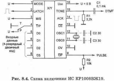
On fig. 8.4. the connection diagram of the IS KR1008VZH19 is shown. Inputs DO-D3, LATCH and ASK output are connected to the microcontroller. The TONE output is connected to the DTMF signal amplifier, and the DP to the pulse key. If the IC UM91531 is used, then capacitors C2 and C3 can be omitted.
On fig. 8.5 shows the connection diagram of the IS KR1008VZH19 as a dialer. To convert keyboard signals into binary code, the priority encoder IC 8-3 K556IV1 is used. When one of the keyboard buttons "0" - "7" is pressed, a binary code of this digit is formed at the outputs A0 - A3 (pins 9, 7, 6). Logical elements DD2.4 - DD2.6 invert it and feed it to the inputs D0 - D2 of the IC KR1008VZH19. At the output of the GS IS K555IV1 (pin 14), at the moment the keyboard button is pressed, the level changes from "high" to "low", and at the output of the inverter DD2.3 from "low" to "high". Changing the level from "low" to "high" at the input LATCH loads the binary code at the inputs D0 - D3. At the moment the keyboard button is released, the reverse level change at the GS output of the IC K555IV1 and at the LATCH input of the IC KR1008VZH19 leads to dialing a number at the TONE or DP output (depending on the position of the SA1 switch). From the moment the binary code is loaded until the end of the dialing of the digit, the VD1 LED is on. While the VD1 LED is on, dialing the next digit is not possible. If switch SA2 is switched to the open state, then this will allow a set of numbers greater than 7.

(click to enlarge)
In the test mode, IC KR1008VZH19 allows you to perform tone and pulse dialing at a much higher speed. If the state of the M/S input is changed while the CE chip sample input (pin 13) is in the active (low) state, the test mode is enabled. The IC remains in test mode until disabled. Pulse dialing in test mode is 48 times faster (at 480 Hz). Tone dialing is 8 times faster (duration of tone burst and pause between tone bursts is 8,75 ms). In this case, the lower and upper frequency groups are separated by the TONE and DP outputs. For the numbers 0, 1, 6, 8, the TONE output will have a signal with the frequency of the lower group of the two-frequency message, and the DP output will have the upper one. For numbers 2, 3, 4, 5, 8, 9, *, #, A, B, C, D, the signal with the frequency of the upper group will be present at the TONE output, and the lower group at the DP output. A sinusoidal signal is supplied to the TONE output, and rectangular pulses of the corresponding frequency are supplied to the DP output.
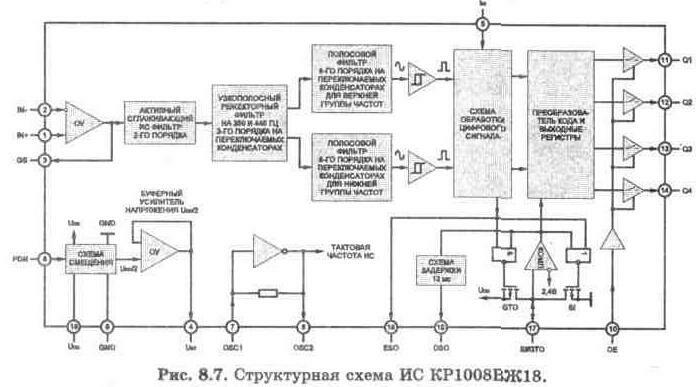
The KR1008VZh18 microcircuit is a receiver - decoder of a two-tone (DTMF) signal (code 2 of 8). The IC is manufactured in a plastic case type 2104.18-A (DIP-18) using CMOS technology and contains band-pass filters on switched capacitors. The microcircuit controls the duration of incoming two-tone messages and pauses between them. The output information is displayed in the form of a 4-bit binary code. The microcircuit is clocked by a quartz oscillator.
Main characteristics of IS KR1008VZH18
- Detection of all 16 standard DTMF signals.
- Low power consumption: 15 mW.
- Single power supply: 5V+5%.
- A standard television quartz resonator with a frequency of 3,579545 MHz is used.
- Tri-state outputs.
- Power down mode in inactive state.
- Low probability of decoding error: 1/10000.
The main areas of application of IS KR1008VZH18
- PBX receivers.
- Paging signal transmission systems.
- Remote control systems.
- credit card systems.
- Pagers.
- Autoresponders.
- Household automatic systems.
- Mobile radio systems.
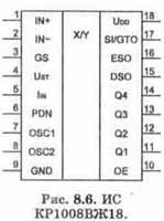
The IC pinout is shown in fig. 8.6, assignment of conclusions in table. 8.5, block diagram in fig. 8.7. Electrical and temporal characteristics are given in table. 8.6. Timing diagrams of inputs and outputs are shown in fig. 8.8, the parallel code at the outputs Q1 - Q4, corresponding to the input two-tone (DTMF) signal, - in table. 8.7.
(click to enlarge)
Tab. 8.5. Pin assignment of IS KR1008VZH18
| Hack and predictor Aviator |
designation |
appointment |
| 1 |
IN+ |
Non-inverting input of the operational amplifier. |
| 2 |
IN- |
Inverting input of the operational amplifier. |
| 3 |
GS |
Operational amplifier output. Used to connect a resistor that sets the gain of the operational amplifier. |
| 4 |
UST |
Reference voltage output (U/2). Can be used to offset op-amp inputs. |
| Hack and predictor Aviator |
designation |
appointment |
| 5 |
II |
Prohibition entry. ' * "High" level on this input disables DTMF signal decoding. |
| 6 |
PDN |
Input for setting the power down mode. The reduction in power consumption occurs at a "high" level at this input. |
| 7 |
OSC1 |
Clock input. An inexpensive 3,579545 quartz resonator connected to the OSC1 and OSC2 pins provides the internal oscillator. (In some cases, for IC KR1008VZH18, it is necessary to install 30 pF capacitors between the clock outputs of the generator and the common wire). You can also apply an external clock directly to the clock input. |
| 8 |
OSC2 |
clock output. |
| 9 |
GND |
General conclusion. |
| 10 |
OE |
Data output enable input. Outputs Q1 - Q4 are CMOS switches that are open when the OE input is "high" and closed (in a high impedance state) when the OE input is "low". |
| 11 12 13 14 |
Q1 Q2 Q3 Q4 |
Tri-state data outputs. When the outputs are open (OE = "1"), they are presented with a binary code corresponding to the last received tone signal (Table 8.7). |
| 15 |
DSO |
Delayed control output. The duration of the output signal ("high" level) at this output corresponds to the duration of the tone signal received at the input of the IC. A "high" level is present from the moment the DTMF signal is recognized (at least 40 ms long) and the decoded binary code arrives at data outputs Q1 - Q4. The DSO output returns to a "low" state when the voltage at pin 17 (SI/GTO) falls below the SI control input threshold (UTS=2,4V at UDD=5V (see Figure 8.8). |
| 18 |
ESO |
Early control exit. This output is immediately "high" when the DTMF signal is recognized by the digital signal processing circuit (Figure 8.7). Any momentary loss of the DTMF signal causes the ESO output state to return to a "low" level. |
| 17 |
SI/GTO |
Bidirectional: Control input/Set time setting output. When the voltage at this input is above the UTS level (2,4 V at UDD = 5 V), the DTMF signal is processed according to the digital algorithm of the IC, and the state of the 4-bit data code outputs (Q1 - Q4) is updated. When the voltage is below UTN, the IC registers are freed to accept a new signal, and the state of the outputs Q1 - Q4 does not change. Using external elements on the GTO output, you can set the timing parameters for processing the DTMF signal, and its state is determined by the functioning of the ESO output and the voltage at the SI input (see Fig. 8.8). |
| 18 |
UDD |
Power plus (+5 V). |

Maximum permissible characteristics. IS CR1008VZH18
Maximum supply voltage (UDD) .................... 6 V.
Analog signal input voltage (UINA) ....... -0,3 V to (UDD + 0,3) V.
Digital signal input voltage (UIND) ......... -0,3 V to (UDD + 0,3) V.
Maximum continuous input current for any output (1m) .......... 10 mA.
Operating temperature (TOPR) ............................................... .. from -40 C to +85 C.
Storage temperature (TSTG) ................................................ from - 60 C to +15 C.
Tab. 8.6. Electrical and timing characteristics of IC KR1008VZH18
| Parameters |
designation |
Value |
Measurement mode |
| min |
a type. |
max |
| Supply voltage |
UDD |
4,75G.75 |
5,0 |
5,25 |
|
| Consumption current, mA |
IDD |
|
3,0 |
9,0 |
PDN="0" |
| Storage current, uA |
IDDQ |
|
10 |
25 |
PDN="1" |
| Power consumption, mW |
PD |
|
15 |
45 |
PDN="0" |
| Input voltage "high" level, V |
Uih |
3,5 |
|
|
UDD = 5V |
| Input voltage "low" level, V |
UIL |
|
|
1,5 |
UDD=5B |
| Input leakage current, μA |
IIH/IIL |
|
0,1 |
|
UIN = 0V or UDD |
| OE output input current, uA |
IOEI |
|
7,5 |
20 |
OE=0B, UDD=5B |
| Input impedance of analog input, MΩ |
RI |
|
10 |
|
fiN = 1 kHz |
| Threshold voltage of control input SI, V |
UTS |
2,2 |
2,4 |
2,5 |
UDD=5B |
| Output voltage "low" level, V |
UOL |
|
|
0,03 |
|
| Output voltage "high" level, V |
UOH |
UDD-0,03 |
|
|
|
| Output current "low" level, mA |
IOL |
1,0 |
2,5 |
|
UOL=0,4V |
| Output current "high" level, V |
IOH |
0,4 |
0,8 |
|
UOH = 4,6V |
| Output reference voltage at the output UST, V |
UST |
2. 3 |
2,5 |
2,7 |
UDD= 5V |
| Output impedance of UST output, Ohm |
ROR |
|
1 |
|
|
| Input signal level (each tone of a two-tone message), dB |
UI |
-29 |
|
+1 |
|
| Input signal level (each tone of a two-tone message), mV |
UI |
27,5 |
|
869 |
|
| Tone deviation |
f |
|
|
+1,5% +2Hz |
|
| Duration of tone signal processing, ms |
tREC |
20 |
|
40 |
Installed by external elements |
| Interdigit pause processing time, ms |
tID |
20 |
|
40 |
Installed by external elements |
| Tone identification time, ms |
tDP |
6 |
11 |
14 |
|
| Interdigit pause identification time, ms |
tDA |
0,5 |
4 |
8,5 |
|
Tab. 8.7. Parallel code at the outputs Q1 - Q4 of the IC KR1008VZh18, corresponding to the input two-tone (DTMF) signal
On fig. 8.9 shows the connection diagram of the IS KR1008VZH18. The input DTMF signal through the coupling capacitor C1 and the resistor R1 is fed to the inverting input IN- operational amplifier. OA gain Ku = R2/R1 (for this circuit Ku = 1). To bias the input of the op-amp, a voltage of 2,5 V is applied from the output of Ust to the non-inverting input IN+. The input impedance of the circuit is approximately equal to the resistance R1. If the quartz resonator ZQ1 is installed directly at the OSC1 and OSC2 terminals, and the generator is stable, then the capacitors C2 and C3 can be omitted.
The duration of the output signal ("high." level) at the output of the DSO (pin 15) corresponds to the duration of the tone signal received at the input of the IC. This output is "high" from the moment the DTMF signal is recognized and the decoded binary code arrives at data outputs Q1 - Q4. The DSO output returns to the "low" state after the inter-digit pause has been recognized and processed (see Figure 8.8).
Resistor R3 and capacitor C4, connected to the ESO and SI/GTO pins, set the minimum duration of the processing of a tone signal or pause after the signal or inter-digit pause has been recognized:
- tone signal processing duration tGTP = 0,875xR4xC26 (XNUMX ms);
- the duration of processing the inter-digit pause tGTA = 0,956xR3xC4 (29 ms).

Duration of tone signal processing and interdigital pause for the scheme of fig. 8.9 are approximately equal. If the duration of the tone signal is longer than the inter-digit pause, then it is possible. connect external elements as shown in fig. 8.10a. If the duration of the tone signal is less than the inter-digit pause, then it is recommended to connect external elements according to fig. 8.106.
For the scheme of Fig. 8.10a:
tGTP=0,875xR1xC;
tGTA= 0,956x[R1xR2/(R1+R2)]C.
For the scheme of Fig. 8.106:
tGTP= 0,875x[R1xR2/(R1+R2)]xC;

tGTA=0,956xR1xC.
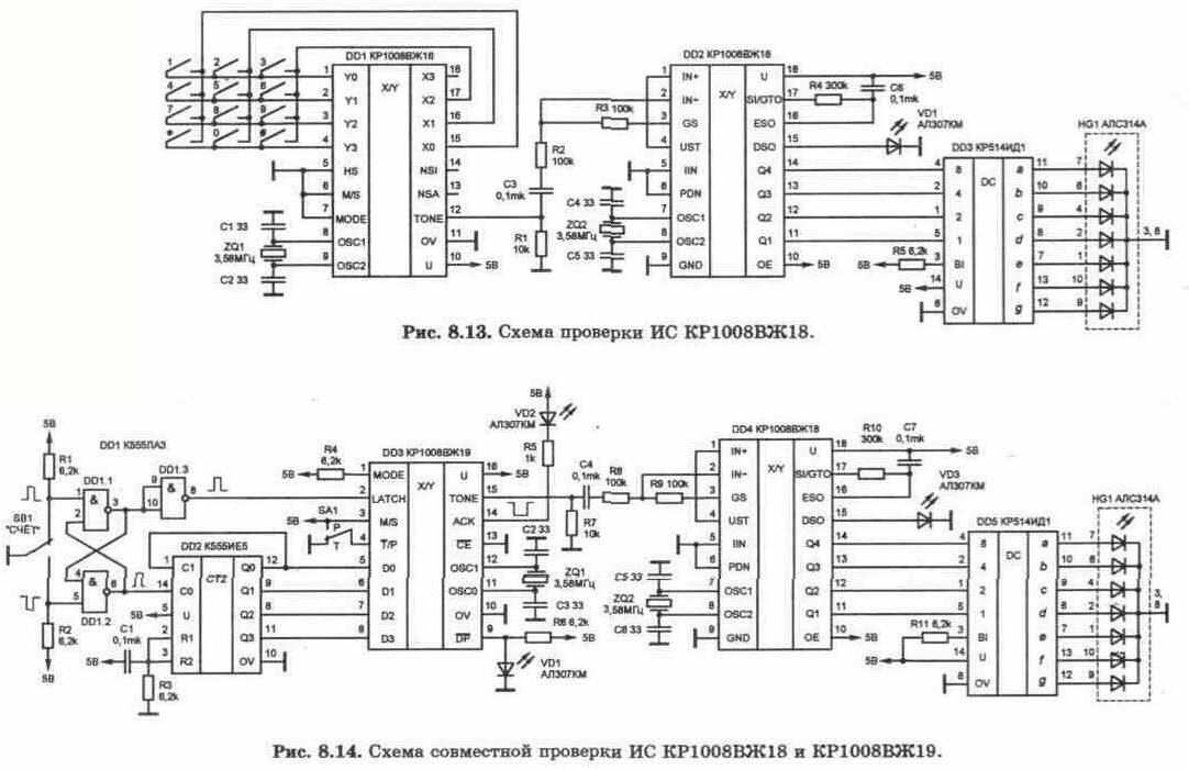
Ha fig. 8.13 shows the scheme for checking IS KR1008VZH18. IC KR1008VZH16 is used as a tone dialer. When you press any dialer button from the TONE output (pin 12) through the C3 DTMF isolation capacitor, the signal is fed to the input of the OU IC KR1008VZH18. The tone signal is decoded and a 4-bit binary code (Table 8.7), corresponding to the input DTMF signal, is fed to inputs 1, 2, 4, 8 of the KR514ID1 decoder. From the moment of identification and until the end of the tonal message, the VD1 LED is on. Outputs a - g of the decoder are connected to a seven-segment LED indicator.
The symbol on the indicator corresponds to the penultimate column of the table. 8.7. The decoder KR514ID1 contains internal current-limiting resistors (Iout. = 5 mA), which allows you to connect indicators with a common cathode AJI304A (B, C), ALS314A directly to the outputs of the decoder. To use indicators with a common anode (ALS324B, ALS3ZZV.G, etc.), you should use the decoder KR514ID2 (Fig. 8.11) or K555ID18. Since the outputs of the IC KR514ID2 are made on open-collector transistors, it is necessary to install limiting resistors with a resistance of 300 ohms. The circuit can be simplified by using the controlled indicator IC with the K490IP2 decoding circuit (Fig. 8.12).
On fig. 8.14 shows a scheme for joint verification of IS KR1008VZH19 and KR1008VZH18. In the initial state, the output of the logic elements DD1.2, DD1.3 and the outputs Q0 - Q3 of the decimal counter DD2 K555IE5 is a "low" level, and the output of the ASC IS KR1008VZH19 is a "high" level. Circuit C1, R3, when the circuit is turned on, sets the outputs of IC DD2 to the state of logical "0". When you press the SB1 button, the outputs DD1.2 and DD1.3 go from "low" to "high" and the IC KRYU08VZH19 loads the binary code through the inputs D0 - D3. At the moment the button is released, the RS-trigger on the logical elements DD1.1 and DD1.2 is flipped back, which leads to the dialing of the loaded digit and moves the counter DD2 forward one cycle. Tone signal "*" from the TONE output of IC KRYU08VZH19 goes to the input of IC KR1008VZH18 and the symbol of the decoded signal is displayed on the HGI indicator (Table 8.7). From the moment the binary code is loaded until the end of dialing, the VD2 LED is on. The next time you press the SB1 button, the next digit "1" is dialed, etc. If the switch SA1 is in the "P" position, then when the next digit is dialed, the VD1 LED flashes with a pulse dialing frequency of 10 Hz. The number of pulses corresponds to the dialed digit.


(click to enlarge)
Publication: cxem.net
 See other articles Section Telephony.
Read and write useful comments on this article.
<< Back
 Latest news of science and technology, new electronics:
Artificial leather for touch emulation
15.04.2024
In a modern technology world where distance is becoming increasingly commonplace, maintaining connection and a sense of closeness is important. Recent developments in artificial skin by German scientists from Saarland University represent a new era in virtual interactions. German researchers from Saarland University have developed ultra-thin films that can transmit the sensation of touch over a distance. This cutting-edge technology provides new opportunities for virtual communication, especially for those who find themselves far from their loved ones. The ultra-thin films developed by the researchers, just 50 micrometers thick, can be integrated into textiles and worn like a second skin. These films act as sensors that recognize tactile signals from mom or dad, and as actuators that transmit these movements to the baby. Parents' touch to the fabric activates sensors that react to pressure and deform the ultra-thin film. This ... >>
Petgugu Global cat litter
15.04.2024
Taking care of pets can often be a challenge, especially when it comes to keeping your home clean. A new interesting solution from the Petgugu Global startup has been presented, which will make life easier for cat owners and help them keep their home perfectly clean and tidy. Startup Petgugu Global has unveiled a unique cat toilet that can automatically flush feces, keeping your home clean and fresh. This innovative device is equipped with various smart sensors that monitor your pet's toilet activity and activate to automatically clean after use. The device connects to the sewer system and ensures efficient waste removal without the need for intervention from the owner. Additionally, the toilet has a large flushable storage capacity, making it ideal for multi-cat households. The Petgugu cat litter bowl is designed for use with water-soluble litters and offers a range of additional ... >>
The attractiveness of caring men
14.04.2024
The stereotype that women prefer "bad boys" has long been widespread. However, recent research conducted by British scientists from Monash University offers a new perspective on this issue. They looked at how women responded to men's emotional responsibility and willingness to help others. The study's findings could change our understanding of what makes men attractive to women. A study conducted by scientists from Monash University leads to new findings about men's attractiveness to women. In the experiment, women were shown photographs of men with brief stories about their behavior in various situations, including their reaction to an encounter with a homeless person. Some of the men ignored the homeless man, while others helped him, such as buying him food. A study found that men who showed empathy and kindness were more attractive to women compared to men who showed empathy and kindness. ... >>
| Random news from the Archive Intel Solar Powered
30.11.2011
Intel has taken another step towards increasing the energy efficiency of processors. The first prototype of a tiny Claremont chip, powered by a small solar array, was demonstrated at the Intel Developer Forum in San Francisco.
In the lowest power consumption mode, the new processor required only 10 mW of electricity to operate.
|
Other interesting news:
▪ Allen-Bradley CompactLogix 1769 programmable controller
▪ New IEEE 802.15.4 Transceiver CC2520 for ZigBee Networks
▪ The thinnest 13-megapixel module from Toshiba
▪ Electric car that absorbs carbon dioxide
▪ Jaw movement generates electricity
News feed of science and technology, new electronics
 Interesting materials of the Free Technical Library:
▪ section of the website Experiments in Physics. Selection of articles
▪ article Myth about television operators. video art
▪ Article What blunder did Nike make when shooting a sneaker ad featuring an African tribe? Detailed answer
▪ article Walking oars. Personal transport
▪ article Why are you making noise at me in vain, birches? Encyclopedia of radio electronics and electrical engineering
▪ article Coins from a magic wand. Focus Secret
Leave your comment on this article:
 All languages of this page
Home page | Library | Articles | Website map | Site Reviews

www.diagram.com.ua
2000-2024


 Arabic
 Bengali
 Chinese
 English
 French
 German
 Hebrew
 Hindi
Hindi Italian
 Japanese
 Korean
 Malay
Malay Polish
 Portuguese
 Spanish
 Turkish
 Ukrainian
 Vietnamese


