|
|


 Arabic
 Bengali
 Chinese
 English
 French
 German
 Hebrew
 Hindi
Hindi Italian
 Japanese
 Korean
 Malay
Malay Polish
 Portuguese
 Spanish
 Turkish
 Ukrainian
 Vietnamese
|
ENCYCLOPEDIA OF RADIO ELECTRONICS AND ELECTRICAL ENGINEERING Stereo modulators for FM. Encyclopedia of radio electronics and electrical engineering
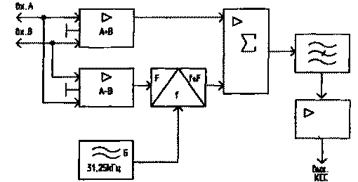
Encyclopedia of radio electronics and electrical engineering / Miscellaneous electronic devices In many imported radio tape recorders there is no input for recording from external devices. The magazine "Radio Amateur" provided diagrams of small VHF transmitters that provide the ability to record from external devices over the air. But in this case, the recording is monophonic. I offer simple stereo modulator circuits for the domestic standard with polar modulation, for the European standard with a pilot tone, and, finally, a "combined" modulator, since the same nodes are used in both circuits. Polar modulation system. Schematic diagram of the modulator is shown in fig. 1, and structural - to explain the principle of its operation - in Fig.2.
Signals from two sources A and B (Fig. 2) are added and subtracted in the corresponding blocks. The total (A + B) signal passes directly to the adder, and the difference (A-B) - modulates the amplitude of the subcarrier frequency (31,25 kHz) generated by the generator G. Further, the total (A + B) signal and amplitude modulated by the difference signal The (A-B) subcarrier frequencies are added together and fed to a notch filter that 5 times (-14 dB) suppresses the subcarrier frequency level. After the filter, a complex stereo signal (CSS) is fed to the modulator of the VHF transmitter.
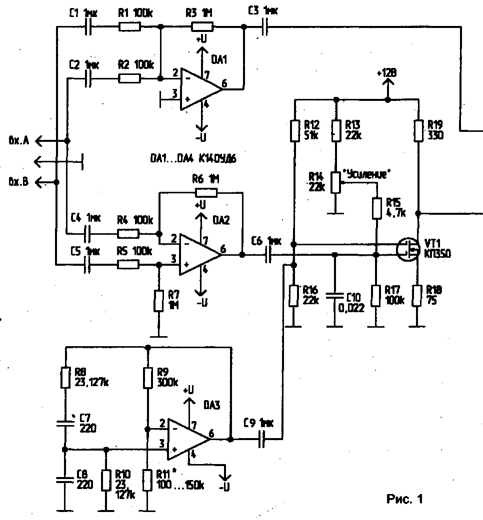
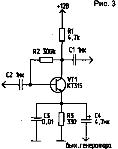
An adder and a differential amplifier are assembled on operational amplifiers DA1, DA2 (Fig. 1) (summation and subtraction of signals A and B). A 3 kHz subcarrier generator is assembled on the DA31,25 op amp. Transistor VT1 - amplitude modulator. Instead of a double-gate field-effect transistor, a cascade can be used, the circuit of which is shown in Fig. 3.
The DA4 op amp implements a signal adder circuit (A + B) and an amplitude modulated subcarrier. From the DA4 output, the signal is fed to a notch filter (L1, C 13), which is an LC circuit with a quality factor of 100 ± 5. The bandwidth of such a circuit reaches 312,5 Hz. At the same time, the lower frequencies of the sidebands of the difference signal (A-B) are attenuated. The residual frequency deviation of the subcarrier transmitter is ±10 kHz, and the maximum deviation of the complex stereo signal is 40 kHz [1]. From the output of the buffer amplifier to VT2, the KSS is fed to the modulator of the FM transmitter. European standard. The functional diagram of the modulator is shown in Fig. 4, the principal - in Fig. 5 [2].
As well as in the domestic standard, from two input signals A and B (Fig. 4) their sum and difference are obtained. The difference signal modulates the 38 kHz subcarrier using a balanced modulator. The subcarrier generator (G) operates at half frequency (19 kHz). Further, the sum signal (A + B), the sidebands of the difference (A-B) signal and the generator frequency (pilot tone) 19 kHz are fed to the summing amplifier (E), from the output of which the complex stereo signal of the KSS is fed to the FM transmitter modulator.
On OS DA1. DA2, DA3 (Fig. 5) summing and differential amplifiers and a pilot tone generator (19 kHz) are assembled. A balanced modulator is assembled on transistors VT1, VT2, doubling the frequency of the generator [3]. The carrier amplitude is chosen to be slightly larger than necessary to start clipping. The shape of the output current is a limited sinusoid. When symmetrically limited, it contains only the odd harmonics of the carrier. When a modulating signal arrives at the other input, clipping becomes unbalanced. and the second harmonic appears in the output current. The LI, C11 circuit must be tuned to the second harmonic. The output of the modulator is a DSB signal. The trimmer resistor R16 balances the modulator, achieving a minimum output signal in the absence of modulation. A summing amplifier is assembled on DA4, from the output of which the KSS is fed to the modulator of the FM transmitter. After the summing amplifier (point A), a delay line can be connected to compensate for the signal delay in the balanced modulator (not shown in the diagram in Fig. 5). Since both modulators have the same nodes, it is possible to create a "universal" modulator immediately for domestic and European standards. Its scheme is shown in Fig.6.
The calculation of circuit elements is given in [4]. As an op amp, you can use any with a large input impedance. Literature
Author: A. Ilyin, St. Petersburg; Publication: N. Bolshakov, rf.atnn.ru
Alcohol content of warm beer
07.05.2024 Major risk factor for gambling addiction
07.05.2024 Traffic noise delays the growth of chicks
06.05.2024
▪ A new way to pasteurize milk ▪ Electric turbines from Formula 1 for road cars ▪ ARCHOS launches ultra-compact audio player with 3 GB hard drive
▪ section of the site for the radio amateur-designer. Article selection ▪ article Pathetic words. Popular expression ▪ article White step. Legends, cultivation, methods of application ▪ article VHF Frequency Synthesizer. Encyclopedia of radio electronics and electrical engineering ▪ article Competition of two pencils. physical experiment
Home page | Library | Articles | Website map | Site Reviews
www.diagram.com.ua |


 Leave your comment on this article: