Chips for household equipment M24C128, M24C256, M24C32, M24C64, M24C16, TDA7318, TDA7309, TDA7313. Reference data

Encyclopedia of radio electronics and electrical engineering / Application of microcircuits
 Comments on the article
Non-volatile memory chips
М24С128, М24С256
Chips М24С128 and М24С256 are electrically reprogrammable ROM (EEPROM) with access via serial interface I2With a capacity of 128 and 256 kbps, respectively. They are used in a wide range of applications.
The main characteristics and functions of microcircuits:
- Serial access I2C with clock frequency up to 400 kHz.
- Supply voltage range:
- 4,5...5,5 V (M24S128, MS24S256)
- 2,5...5,5 V (M24C128-W, M24C256-W).
- The possibility of hardware write protection is provided.
- Ability to write a byte or page (up to 64 bytes).
- Reading is performed with random or sequential access.
- Provided at least 105 read/write cycles.
- The information storage period is not less than 40 years.
The memory of microcircuits is organized as an array of 32768x8 bits (M24S256) and 16384x8 bits (M24S128). They are available in eight-pin packages PSDIP-8, SO-8, TSS0P-8.
The purpose of the pins of the microcircuits is shown in Table. 1, and their location is shown in Fig. one.

Fig. 1
Table 1
| Output No. |
Signal |
Description |
| 1 |
NC |
Not used |
| 2 |
NC |
Not used |
| 3 |
NC |
Not used |
| 4 |
vss |
General |
| 5 |
SDA |
Interface data line I2C |
| 6 |
SCL |
I interface clock line2C |
| 7 |
WC |
Write disable input |
| 8 |
Vcc |
Food |
The microcircuits include an initial reset circuit when a supply voltage is applied to them.
Electrical parameters
The consumption currents of microcircuits at various supply voltages have the following values:
voltage 5 V |
2 mA |
| voltage 2,5V (-W) |
1 mA |
| voltage 1,8V (-S) |
0,8 mA |
| Synchronization frequency in all cases |
400 kHz |
| The data recording time is no more than |
10 ms |
M24C32, M24C64
Microcircuits М24С32 and М24С64 are electrically reprogrammable ROMs with access via serial interface I2With a capacity of 32 and 64 kb, respectively. They are used in a wide range of applications.
The main characteristics and functions of microcircuits:
- Serial access I2C with clock frequency up to 400 kHz.
- Supply voltage range:
- 4,5...5,5 V (M24S32, M24S64)
- 2,5...5,5 V (M24C32-W, M24C64-W)
- 1,8...3,6 V (M24C32-S, M24C64-S).
- The possibility of hardware write protection is provided.
- Ability to write a byte or page (up to 32 bytes).
- Reading is performed with random or sequential access.
- Provides at least 106 read/write cycles.
- The information storage period is not less than 40 years.
The memory of microcircuits is organized as an array of 8192x8 bits (M24C64) and 4096x8 bits (M24C32). They are available in eight-pin packages PSDIP-8, SO-8, TSS0P-8.
The purpose of the pins of the microcircuits is shown in Table. 2, and their location is shown in Fig. one.

Fig. 2
Table 2
| Output No. |
Signal |
Description |
| 1 |
EO |
Chip select bit 0 |
| 2 |
E1 |
Chip select bit 1 |
| 3 |
E2 |
Chip select bit 2 |
| 4 |
vss |
General |
| 5 |
SDA |
Interface data line I2C |
| 6 |
SCL |
I interface clock line2C |
| 7 |
WC |
Write disable input |
| 8 |
Vcc |
Food |
To Bus I2C, up to 8 M24C32 (M24C64) chips can be connected. Inputs E0-E2 are used to set the hardware address of the microcircuit. The chip compares the logic levels of these inputs with the least significant three bits in the device select byte.
The WC input is used for hardware (permanent or dynamic) prohibition of data writing to the chip.
The microcircuits include an initial reset circuit when the supply voltage is applied.
Electrical parameters
The consumption currents of microcircuits at various supply voltages have the following values:
voltage 5 V |
2 mA |
| voltage 2,5V (-W) |
1 mA |
| voltage 1,8V (-S) |
0,8 mA |
| Synchronization frequency in all cases |
400 kHz |
| The data recording time is no more than |
10 ms |
M24S16
The M24C16 chip is an electrically reprogrammable ROM with access via a serial interface I2With a capacity of 16 kb. It is used in a wide range of applications.
The main characteristics and functions of the microcircuit:
- Serial access I2C with clock frequency up to 400 kHz.
- Supply voltage range:
- 4,5...5,5V(M24C16)
- 2,5.3,5V (M24C16-W)
- 1,8..5,5 V (M24C16-R)
- 1.8-3,6V (M24C16-S).
- The possibility of hardware write protection is provided.
- Ability to write a byte or page.
- Reading is performed with random or sequential access.
- Provided at least 106 read/write cycles.
- The information storage period is not less than 40 years.
The chip memory is organized as a 2048x8 bit array. It is available in eight-pin packages PSDIP-8, SO-8, TSS0P-8.
The purpose of the pins of the microcircuit is shown in Table. 3, and their location is shown in Fig. one.
Table 3
| Output No. |
Signal |
Description |
| 1 |
NC |
Not used |
| 2 |
NC |
Not used |
| 3 |
NC |
Not used |
| 4 |
vss |
General |
| 5 |
SDA |
Interface data line I2C |
| 6 |
SCL |
I interface clock line2C |
| 7 |
WC |
Write disable input |
| 8 |
Vcc |
Food |
The WC input is used for hardware (permanent or dynamic) prohibition of data writing to the chip.
Electrical parameters
The current consumption of the microcircuit at various supply voltages and synchronization frequencies has the following values:
voltage 5 V,
clock frequency 400 kHz |
2 mA |
| voltage 2,5 V (-W), frequency 400 kHz |
1 mA |
| voltage 1,8 V (-R), frequency 100 kHz |
0,8 mA |
| voltage 1,8 V (-S), frequency 400 kHz |
0,8 mA |
| The data recording time is no more than |
10 ms |
Sound Processor Chips
TDA7318
Four-channel sound processor TDA7318 with digital control on the bus I2C is used in audio equipment for a wide range of applications.
Key Features and Functions
- It includes a built-in audio signal input selector (multiplexer) 4 to 1 (stereo) with an adjustable preamplifier.
- Output to two stereo channels (front and rear).
- Volume control is provided in 1,25 dB steps.
- Separate adjustment of the level of wind and low frequencies is provided.
- It is possible to separately adjust the volume for the right and left channels, for the front and rear.
- The processor is controlled via a serial digital bus I2C.
The microcircuit is made in a DIP-28 package. The block diagram of the processor is shown in fig. 3. The location of the pins of the microcircuit is shown in fig. 4.
The purpose of the pins of the microcircuit is presented in Table. four.
Table 4
| Output No. |
Signal |
Description |
| 1 |
CREF |
External correction circuit |
| 2 |
VDD |
Supply voltage |
| 3 |
GND |
General |
| 4 |
TREBEL |
Left channel treble correction circuit |
| 5 |
TREBLE R |
Right channel treble correction circuit |
| 6 |
IN(R) |
Input (right channel) |
| 7 |
OUT(R) |
Multiplexer output (right channel) |
| 8 |
RIGHT INPUT 4 |
Multiplexer input 4 (right channel) |
| 9 |
RIGHT INPUT 3 |
Multiplexer input 3 (right channel) |
| 10 |
RIGHT INPUT 2 |
Multiplexer input 2 (right channel) |
| 11 |
RIGHT INPUT 1 |
Multiplexer input 1 (right channel) |
| 12 |
LEFT INPUT 4 |
Multiplexer input 4 (left channel) |
| 13 |
LEFT INPUT 3 |
Multiplexer input 3 (left channel) |
| 14 |
LEFT INPUT 2 |
Multiplexer input 2 (left channel) |
| 15 |
LEFT INPUT 1 |
Multiplexer input 1 (left channel) |
| 16 |
IN(L) |
Input (left channel) |
| 17 |
OUT(L) |
Multiplexer output (left channel) |
| 18 |
BASS BIN(L) |
Bass correction circuit (left channel) |
| 19 |
BASS BOUT(L) |
Bass correction circuit (left channel) |
| 20 |
BASS BIN(R) |
Bass correction circuit (right channel) |
| 21 |
BASS BOUT(R) |
Bass correction circuit (right channel) |
| 22 |
OUTRR |
Output, rear right channel |
| 23 |
OUTLR |
Output, rear left channel |
| 24 |
OUTRF |
Output, front right channel |
| 25 |
OUT LF |
Output, front left channel |
| 26 |
BUS DIG GND |
Common Interface I2С |
| 27 |
BUS SCL |
I interface clock line2С |
| 28 |
BUS SDA |
Interface data line I2C |

Fig. 3

Fig. 4
If a signal is supplied to the processor input from only one source (the use of an input multiplexer is not required), then the elements C1-C8 are excluded, and the signal is applied to the left (according to the diagram in Fig. 3) conclusions of the capacitors C10 and C11, which are disconnected, respectively, from the pin. 7 and 17 chips.
Electrical parameters
| Nonlinear distortion factor at a frequency of 1 kHz,% |
0,01 |
| Signal-to-noise ratio, dB |
106 |
| Channel separation at a frequency of 1 kHz, dB |
100 |
| Output signal level in MUTE mode, dB |
-100 |
| Output level adjustment step, dB |
1,25 |
| Output signal level adjustment range, dB |
-78,5...0 |
| Tone control step, dB |
2 |
| Tone control range at low and high frequencies, dB |
±14 |
| Balance adjustment step, dB |
1,25 |
| Balance and offset adjustment range, dB |
-38,75...0 |
| Input selector gain adjustment step, dB |
6,25 |
| Input selector gain adjustment range, dB |
0 18,75 ... |
| Input impedance (selector inputs), kOhm |
50 |
| Input impedance (regulator inputs), kOhm |
33 |
| Volume control range, dB |
75 |
| Load resistance at the output, not less than, kOhm |
2 |
| Maximum permissible parameters |
| Supply voltage, V |
6 10 ... |
| Consumption current, mA |
4 11 ... |
| Maximum input signal level, V |
2 |
| Ambient temperature, ° С |
-40...85 |
TDA73O9
Dual-channel sound processor TDA7309 with digital control over the I bus2C is used as a multifunctional volume control in audio equipment for a wide range of applications.
Key Features and Functions
- It includes a built-in input selector (multiplexer) 3 to 1 (stereo).
- There are direct outputs from the selector, and there is also a frequency response correction function for low volume mode (loudness).
- Volume control is provided in 1 dB steps.
- Separate adjustment of the level of high and low frequencies is provided.
- It is possible to separately adjust the volume for the right and left channels, as well as smooth sound mute (soft mute).
- The control is carried out via a serial digital bus I2C.
The microcircuit is made in DIP-20 (TDA7309) and SO-20 (TDA7309D) packages.
The location of the pins of the microcircuit is shown in fig. 5.
The block diagram of the processor is shown in fig. 6. The purpose of the pins of the microcircuit is shown in Table. 5.
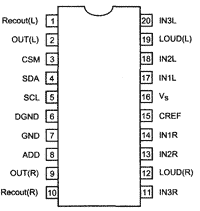
Fig. 5

Fig. 6
Table 5
| Output No. |
Signal |
Description |
| 1 |
Recout(L) |
Left channel direct output |
| 2 |
OUTL |
Left channel output |
| 3 |
CSM |
Time-setting capacitor of the smooth volume reduction unit |
| 4 |
SDA |
Interface data line I2C |
| 5 |
SCL |
I interface clock line2C |
| 6 |
DGND |
Common Interface I2C |
| 7 |
GND |
Signal common wire |
| 8 |
ADD |
Chip address select input |
| 9 |
OUTR |
Right channel output |
| 10 |
Recout(R) |
Right channel direct output |
| 11 |
IN3L |
Input 3 (left channel) |
| 12 |
LOUDL |
Left channel correction circuit |
| 13 |
IN2L |
Input 2 (left channel) |
| 14 |
IN1L |
Input 1 (left channel) |
| 15 |
Vs |
Supply voltage |
| 16 |
CREF |
External correction circuit |
| 17 |
IN1R |
Input 1 (right channel) |
| 18 |
IN2R |
Input 2 (right channel) |
| 19 |
LOUDR |
Right channel correction circuit |
| 20 |
IN3R |
Input 3 (right channel) |
The address selection input (pin 8) sets the chip number if two identical chips are used.
Electrical parameters
(under the following conditions: ambient temperature 25°C, supply voltage 9 V, output load resistance 10 kΩ, all controls set to 0 dB):
| Nonlinear distortion factor at a frequency of 1 kHz,% |
0,01 |
| Signal-to-noise ratio, dB |
106 |
| Channel separation at a frequency of 1 kHz, dB |
100 |
| Output signal level in SOFT MUTE mode, dB |
-60 |
| Output signal level in MUTE mode, dB |
-100 |
| Input resistance, kOhm |
50 |
| Volume control range, dB |
92 |
| Load resistance at the output, not less than, kOhm |
2 |
Maximum permissible parameters
| Supply voltage, V |
10 |
| Consumption current, mA |
no more 10 |
| Maximum input signal level, V |
2 |
| Ambient temperature, ° С |
-40...85 |
TDA7313
Three-channel (stereo) sound processor TDA7313 with digital control on the bus I2C is used in audio equipment for a wide range of applications.
Main characteristics and functions of the processor
- It includes a built-in input selector (multiplexer) of audio signals 3 to 1 (stereo) with an adjustable preamplifier.
- There are outputs for two stereo channels (front and rear), and there is also a frequency response correction function for low volume (loudness).
- The volume is adjusted in steps of 1,25 dB.
- Adjustment of level of high and low frequencies is provided.
- It is possible to separately adjust the volume for the right and left channels, for the front and rear, as well as smooth sound mute (soft mute).
- Serial digital bus control I2C.
The microcircuit is produced in a DIP-28 package. The block diagram of the processor is shown in fig. 7.
The location of the pins of the microcircuit is shown in fig. 8.
The purpose of the pins of the microcircuit is presented in Table. four.

Fig. 7

Fig. 8
Table 6
| Output No. |
Signal |
Description |
| 1 |
CREF |
External correction circuit |
| 2 |
VDD |
Supply voltage |
| 3 |
GND |
General |
| 4 |
TREBLE L |
Left channel treble correction circuit |
| 5 |
TREBLE R |
Purpose of right channel treble correction |
| 6 |
IN(R) |
Input (right channel) |
| 7 |
OUT(R) |
Multiplexer output (right channel) |
| 8 |
LOUD-R |
Right channel loudness circuit |
| 9 |
RIGHT INPUT 3 |
Multiplexer input 3 (right channel) |
| 10 |
RIGHT INPUT 2 |
Multiplexer input 2 (right channel) |
| 11 |
RIGHT INPUT 1 |
Multiplexer input 1 (right channel) |
| 12 |
LOUDL |
Left channel loudness circuit |
| 13 |
LEFT INPUT 3 |
Multiplexer input 3 (left channel) |
| 14 |
LEFT INPUT 2 |
Multiplexer input 2 (left channel) |
| 15 |
LEFT INPUT 1 |
Multiplexer input 1 (left channel) |
| 16 |
IN(L) |
Input (left channel) |
| 17 |
OUT(L) |
Multiplexer output (left channel) |
| 18 |
BASS BIN(L) |
Bass correction circuit (left channel) |
| 19 |
BASS BOUT(L) |
Bass correction circuit (left channel) |
| 20 |
BASS BIN(R) |
Bass correction circuit (right channel) |
| 21 |
BASS BOUT(R) |
Bass correction circuit (right channel) |
| 22 |
OUTRR |
Output, rear right channel |
| 23 |
OUTLR |
Output, rear left channel |
| 24 |
OUTRF |
Output, front right channel |
| 25 |
OUT LF |
Output, front left channel |
| 26 |
BUS DIG GND |
Common Interface I2С |
| 27 |
BUS SCL |
I interface clock line2С |
| 28 |
BUS SDA |
Interface data line I2С |
If a signal is supplied to the processor input from only one source (the use of an input multiplexer is not required), then the elements C1-C6 are excluded, and the signal is applied to the left terminals of the capacitors C8 and C9 according to the circuit, disconnected respectively from the pin. 7 and 17 chips.
Electrical parameters
(under the following conditions: ambient temperature 25°C, supply voltage 9 V, output load resistance 10 kΩ, all controls set to 0 dB):
| Nonlinear distortion factor at a frequency of 1 kHz,% |
0,01 |
| Signal-to-noise ratio, dB |
106 |
| Channel separation at a frequency of 1 kHz, dB |
100 |
| Output signal level in MUTE mode, dB |
-100 |
| Output level adjustment step, dB |
1,25 |
| Output signal level adjustment range, dB |
-78,5...0 |
| Tone control step, dB |
2 |
| Tone control range at low and high frequencies, dB |
±14 |
| Balance and offset adjustment step, dB |
1,25 |
| Balance adjustment range, dB |
~38,75...0 |
| Input selector gain adjustment step, dB |
3,75 |
| Input selector gain adjustment range, dB |
0 11,25 ... |
| Input impedance (selector inputs), kOhm |
50 |
| Input impedance (regulator inputs), kOhm |
33 |
| Volume control range, dB |
75 |
| Load resistance at the output, not less than, kOhm |
2 |
Maximum permissible parameters
| Supply voltage, V |
10 |
| Consumed current no more than, mA |
11 |
| Maximum input signal level, V |
2 |
| Ambient temperature, ° С |
-40...85 |
Publication: cxem.net
 See other articles Section Application of microcircuits.
Read and write useful comments on this article.
<< Back
 Latest news of science and technology, new electronics:
Machine for thinning flowers in gardens
02.05.2024
In modern agriculture, technological progress is developing aimed at increasing the efficiency of plant care processes. The innovative Florix flower thinning machine was presented in Italy, designed to optimize the harvesting stage. This tool is equipped with mobile arms, allowing it to be easily adapted to the needs of the garden. The operator can adjust the speed of the thin wires by controlling them from the tractor cab using a joystick. This approach significantly increases the efficiency of the flower thinning process, providing the possibility of individual adjustment to the specific conditions of the garden, as well as the variety and type of fruit grown in it. After testing the Florix machine for two years on various types of fruit, the results were very encouraging. Farmers such as Filiberto Montanari, who has used a Florix machine for several years, have reported a significant reduction in the time and labor required to thin flowers.
... >>
Advanced Infrared Microscope
02.05.2024
Microscopes play an important role in scientific research, allowing scientists to delve into structures and processes invisible to the eye. However, various microscopy methods have their limitations, and among them was the limitation of resolution when using the infrared range. But the latest achievements of Japanese researchers from the University of Tokyo open up new prospects for studying the microworld. Scientists from the University of Tokyo have unveiled a new microscope that will revolutionize the capabilities of infrared microscopy. This advanced instrument allows you to see the internal structures of living bacteria with amazing clarity on the nanometer scale. Typically, mid-infrared microscopes are limited by low resolution, but the latest development from Japanese researchers overcomes these limitations. According to scientists, the developed microscope allows creating images with a resolution of up to 120 nanometers, which is 30 times higher than the resolution of traditional microscopes. ... >>
Air trap for insects
01.05.2024
Agriculture is one of the key sectors of the economy, and pest control is an integral part of this process. A team of scientists from the Indian Council of Agricultural Research-Central Potato Research Institute (ICAR-CPRI), Shimla, has come up with an innovative solution to this problem - a wind-powered insect air trap. This device addresses the shortcomings of traditional pest control methods by providing real-time insect population data. The trap is powered entirely by wind energy, making it an environmentally friendly solution that requires no power. Its unique design allows monitoring of both harmful and beneficial insects, providing a complete overview of the population in any agricultural area. “By assessing target pests at the right time, we can take necessary measures to control both pests and diseases,” says Kapil ... >>
| Random news from the Archive Water purification and hydrogen production using artificial photocatalysis
23.11.2023
Researchers from the University of Cambridge have unveiled an innovative solar-powered device that can simultaneously convert polluted or ordinary seawater into hydrogen fuel and clean drinking water.
A new device based on solar energy and using artificial photocatalysis represents a significant step in solving global problems with drinking water and fuel, especially in third world countries.
The scientists embedded a photocatalyst that absorbs ultraviolet light onto a nanostructured carbon mesh, which in turn absorbs infrared light. This approach is designed to stimulate the formation of water vapor, which is used by the photocatalyst to produce hydrogen. The porous carbon mesh, treated to repel water, allows the photocatalyst to move freely and remain above the water's surface, minimizing exposure to contaminants. This device configuration also improves solar energy efficiency. Researchers were able to emulate transpiration technology, imitating the process of water moving through a plant and its evaporation from above-ground parts.
The scientists then tested their invention using real open water sources, including the River Cam in central Cambridge and turbid industrial wastewater from paper production. As a result, the device maintained 80% of initial performance even after 154 hours in artificial seawater.
According to the researchers, since the photocatalyst is isolated from contaminants in the water source and remains relatively dry, the device is able to maintain its operational stability over a long period of time.
|
Other interesting news:
▪ New types of acoustic resonators for frequencies of 1,8...2,0 GHz
▪ Lenses that restore vision
▪ Huawei IdeaHub S2 Interactive Panel
▪ Biological magnetoreception
▪ Prolonged stress erases memory
News feed of science and technology, new electronics
 Interesting materials of the Free Technical Library:
▪ section of the site Assembling the Rubik's Cube. Article selection
▪ Article Pharmacology. Crib
▪ article Why does the city of Baden-Baden have such a double name? Detailed answer
▪ article A simple bayonet with a hose. Tourist tips
▪ FAQ article on the TDA7293/7294 chip. Encyclopedia of radio electronics and electrical engineering
▪ article Power supply and electrical networks. Categories of electrical receivers and ensuring the reliability of power supply. Encyclopedia of radio electronics and electrical engineering
Leave your comment on this article:
 All languages of this page
Home page | Library | Articles | Website map | Site Reviews

www.diagram.com.ua
2000-2024


 Arabic
 Bengali
 Chinese
 English
 French
 German
 Hebrew
 Hindi
Hindi Italian
 Japanese
 Korean
 Malay
Malay Polish
 Portuguese
 Spanish
 Turkish
 Ukrainian
 Vietnamese