Field-effect transistors of the KP727 series. Reference data

Encyclopedia of radio electronics and electrical engineering / Reference materials
 Comments on the article
Powerful silicon field-effect transistors KP727A and KP727B with an insulated gate enriched with an n-channel and a built-in reverse-connected protective diode are manufactured using planar epitaxial technology. They are designed to work in secondary power supplies, in regulators, stabilizers and voltage and current converters with continuous and pulse control, in electric motor drive units and other devices of equipment for wide application.
The transistors are housed in a plastic case KT-28 (TO-220) with stamped hard tinned leads and a heat-removing metal flange with a mounting hole (Fig. 1). The mass of the device is no more than 2,5 g. Foreign analogues of transistors: KP727A - BUZ71, KP727B - IRFZ34.

Main characteristics at Tacr.av = 25°C
- Threshold gate-source voltage, V, at a drain current of 0,25 mA and the same gate-source and drain-source voltages for KP727A......2,1...4
- KP727B......2...4
- Drain pulse current, A, not less, with a pulse duration of less than 300 μs and a duty cycle of more than 50, at a gate-source voltage of 10 V for KP727A (drain-source voltage 2V)...... 14
- KP727B(1,8V)......30
- Drain-source resistance of an open transistor, Ohm, no more, with a pulse duration of less than 300 μs and a duty cycle of more than 50, at a gate-source voltage of 10 V for KP727A (drain current 9 A)...... 0,1
- KP727B(18A)......0,05
- Residual drain current, µA, no more, at maximum drain-source voltage and zero gate-source voltage ...... 25
- Gate leakage current, µA, no more, at gate-source voltage +20 V and zero drain-source voltage ...... ± 0,1
- The slope of the characteristic, A / V, not less, with a pulse duration of less than 300 μs and a duty cycle of more than 50, at a drain-source voltage of 25 V for KP727A (drain current 9 A)...... 4
- KP727B(18A)......9,3
- Constant forward voltage on an open protective diode, V, not more, with a pulse duration of less than 300 μs and a duty cycle of more than 50, at zero gate-source voltage for KP727A (current through the diode 28 A)...... 1,8
- KP727B(30A)......1,6
- Thermal resistance transition-housing, °C/W max, for KP727A......3,1
- KP727B ...... 1,7
- Thermal resistance transition - environment, °C / W, no more ...... 62
- Turn-on time*, µs, no more, at a drain-source voltage of 30 V, a drain current of 30 A and an output resistance of the measuring signal source of 9,1 Ohm.....0,14
- Turn-off time*, µs, no more, at a drain-source voltage of 30 V, a drain current of 30 A and an output resistance of the measuring signal source of 9,1 Ohm ...... 0,12
- Input capacitance*, pF, no more, at zero gate-source voltage and drain-source voltage of 25 V at a frequency of 1 MHz ...... 1600
- Output capacitance*, pF, no more, at zero gate-source voltage and drain-source voltage of 25 V at a frequency of 1 MHz ...... 800
- Capacitance*, pF, no more, at zero gate-source voltage and drain-source voltage of 25 V at a frequency of 1 MHz ..... 195
* Reference parameters.
Operating limits
- The highest drain-source voltage, V, for KP727A......50
- KP727B ...... 60
- Maximum gate-source voltage, V ...... ± 20
- The highest direct drain current, A, at a case temperature of 25 ° C for KP727A ...... 14
- KP727B ...... 30
- The highest pulsed drain current, A, at a case temperature of 25 ° C for KP727A ...... 56
- KP727B ...... 120
- The highest constant dissipated power, W, at a case temperature of 25 ° C for KP727A......40
- KP727B ...... 88
- The highest value of the static potential, V.....200**
- Operating temperature range, °С......-55...+150
** III degree of rigidity according to OST 11073.062.
Operation of transistors with two or more limit values of parameters is prohibited. To improve the reliability of the devices, the values of the parameters should not exceed 70% of the maximum allowable.
One-time bending of the leads is allowed no closer than 5 mm from the body with a bending radius of at least 1,5 mm, and the bend line must lie in the plane of the leads. When bending, measures must be taken to prevent the transfer of force to the body. Conclusions cannot be twisted.
The distance from the body to the place of soldering and tinning should not be less than 5 mm. Soldering temperature - not higher than 265°C, soldering time - no more than 4 s, tinning - 2 s.
To reduce the thermal resistance of the transistor case-heat sink, it is recommended to use special pastes, for example, KPT-8 according to GOST 19783. In cases where an insulating gasket should be under the case, its thermal resistance must be taken into account.
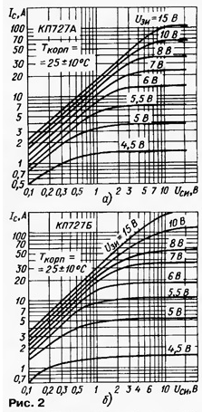
On fig. 2, a and b show typical dependences of the drain current of transistors on the drain-source voltage at normal case temperature, and in fig. 3, a and b - from the gate-source voltage at two values of the junction temperature.

On fig. 4 shows the normalized temperature dependence of the drain-source resistance of an open transistor (Rsi.t25 is the ratio of the current value of the drain-source resistance to the value of this resistance at a junction temperature of 25°C), and in fig. 5 - typical dependences of the input (C11i), output (C22i) and throughput (C12i) capacitance of transistors on the drain-source pulse voltage.


Rice. 6a and XNUMXb illustrate the dependence of the voltage at the terminals of the transistor channel on the current through these terminals, which flows in the direction forward for the protective diode. The main component of this voltage is the voltage drop across the open protective diode.

Author: V.Kiselev
 See other articles Section Reference materials.
Read and write useful comments on this article.
<< Back
 Latest news of science and technology, new electronics:
Traffic noise delays the growth of chicks
06.05.2024
The sounds that surround us in modern cities are becoming increasingly piercing. However, few people think about how this noise affects the animal world, especially such delicate creatures as chicks that have not yet hatched from their eggs. Recent research is shedding light on this issue, indicating serious consequences for their development and survival. Scientists have found that exposure of zebra diamondback chicks to traffic noise can cause serious disruption to their development. Experiments have shown that noise pollution can significantly delay their hatching, and those chicks that do emerge face a number of health-promoting problems. The researchers also found that the negative effects of noise pollution extend into the adult birds. Reduced chances of reproduction and decreased fertility indicate the long-term effects that traffic noise has on wildlife. The study results highlight the need ... >>
Wireless speaker Samsung Music Frame HW-LS60D
06.05.2024
In the world of modern audio technology, manufacturers strive not only for impeccable sound quality, but also for combining functionality with aesthetics. One of the latest innovative steps in this direction is the new Samsung Music Frame HW-LS60D wireless speaker system, presented at the 2024 World of Samsung event. The Samsung HW-LS60D is more than just a speaker system, it's the art of frame-style sound. The combination of a 6-speaker system with Dolby Atmos support and a stylish photo frame design makes this product the perfect addition to any interior. The new Samsung Music Frame features advanced technologies including Adaptive Audio that delivers clear dialogue at any volume level, and automatic room optimization for rich audio reproduction. With support for Spotify, Tidal Hi-Fi and Bluetooth 5.2 connections, as well as smart assistant integration, this speaker is ready to satisfy your ... >>
A New Way to Control and Manipulate Optical Signals
05.05.2024
The modern world of science and technology is developing rapidly, and every day new methods and technologies appear that open up new prospects for us in various fields. One such innovation is the development by German scientists of a new way to control optical signals, which could lead to significant progress in the field of photonics. Recent research has allowed German scientists to create a tunable waveplate inside a fused silica waveguide. This method, based on the use of a liquid crystal layer, allows one to effectively change the polarization of light passing through a waveguide. This technological breakthrough opens up new prospects for the development of compact and efficient photonic devices capable of processing large volumes of data. The electro-optical control of polarization provided by the new method could provide the basis for a new class of integrated photonic devices. This opens up great opportunities for ... >>
| Random news from the Archive Gold red and green
09.11.2012
Scientists from the University of Southampton have found that microscopic manipulation of the surface structure of gold can change its color.
It turns out that thanks to milling using a focused ion beam on the metal surface, it is possible to create nanoscale patterns that have the properties of metamaterials. Scientists managed to form a special pattern on a gold substrate, which changed the reflective properties of gold and visually changed its color. Thus, it is now possible to create red and even green gold. Moreover, this technology is applicable to other metals such as silver and aluminum. This is a completely new approach to painting metals, which does not require the use of carcinogenic dyes.
The pattern on the surface of the metal is only 100 nanometers deep. By selecting a certain depth and pattern of milling, you can control which wavelengths of light the metal absorbs and which reflects. As a result, one metal part can be "painted" in different colors, and with an accuracy that is unattainable with conventional paint. In particular, a silver ring can be decorated with the thinnest stripes of red and green.
Ion beam milling is kind of like sandblasting, but at the atomic level. This technology is well mastered, although it is extremely difficult to paint with it, for example, the skin of a ship. However, it can be used in jewelry and other areas where the creation of surfaces with complex optical properties is required, in particular in promotional items and protected trademarks.
|
Other interesting news:
▪ Space satellite will help in the fight against drought
▪ Raytheon laser systems for detecting and destroying drones
▪ Booking a ticket on the run
▪ The most powerful laser in the world
▪ Wind turbine without blades
News feed of science and technology, new electronics
 Interesting materials of the Free Technical Library:
▪ site section Infrared technology. Article selection
▪ Article Teriya organization. Crib
▪ How are the deaf and dumb taught to speak? Detailed answer
▪ article Wind turbine. Personal transport
▪ article External lightning protection system. Encyclopedia of radio electronics and electrical engineering
▪ article Switchgears and substations with voltages above 1 kV. Oil farm. Encyclopedia of radio electronics and electrical engineering
Leave your comment on this article:
 All languages of this page
Home page | Library | Articles | Website map | Site Reviews

www.diagram.com.ua
2000-2024


 Arabic
 Bengali
 Chinese
 English
 French
 German
 Hebrew
 Hindi
Hindi Italian
 Japanese
 Korean
 Malay
Malay Polish
 Portuguese
 Spanish
 Turkish
 Ukrainian
 Vietnamese